- 您现在的位置:买卖IC网 > PDF目录16259 > DS26324DK (Maxim Integrated Products)KIT DESIGN FOR G549DS26324 PDF资料下载
参数资料
| 型号: | DS26324DK |
| 厂商: | Maxim Integrated Products |
| 文件页数: | 87/120页 |
| 文件大小: | 0K |
| 描述: | KIT DESIGN FOR G549DS26324 |
| 产品培训模块: | Lead (SnPb) Finish for COTS Obsolescence Mitigation Program |
| 标准包装: | 1 |
| 主要目的: | 电信,线路接口单元(LIU) |
| 已用 IC / 零件: | G549DS26324 |
| 已供物品: | 板,线缆,电源 |
第1页第2页第3页第4页第5页第6页第7页第8页第9页第10页第11页第12页第13页第14页第15页第16页第17页第18页第19页第20页第21页第22页第23页第24页第25页第26页第27页第28页第29页第30页第31页第32页第33页第34页第35页第36页第37页第38页第39页第40页第41页第42页第43页第44页第45页第46页第47页第48页第49页第50页第51页第52页第53页第54页第55页第56页第57页第58页第59页第60页第61页第62页第63页第64页第65页第66页第67页第68页第69页第70页第71页第72页第73页第74页第75页第76页第77页第78页第79页第80页第81页第82页第83页第84页第85页第86页当前第87页第88页第89页第90页第91页第92页第93页第94页第95页第96页第97页第98页第99页第100页第101页第102页第103页第104页第105页第106页第107页第108页第109页第110页第111页第112页第113页第114页第115页第116页第117页第118页第119页第120页
DS26324 3.3V, 16-Channel, E1/T1/J1 Short-Haul Line Interface Unit
69 of 120
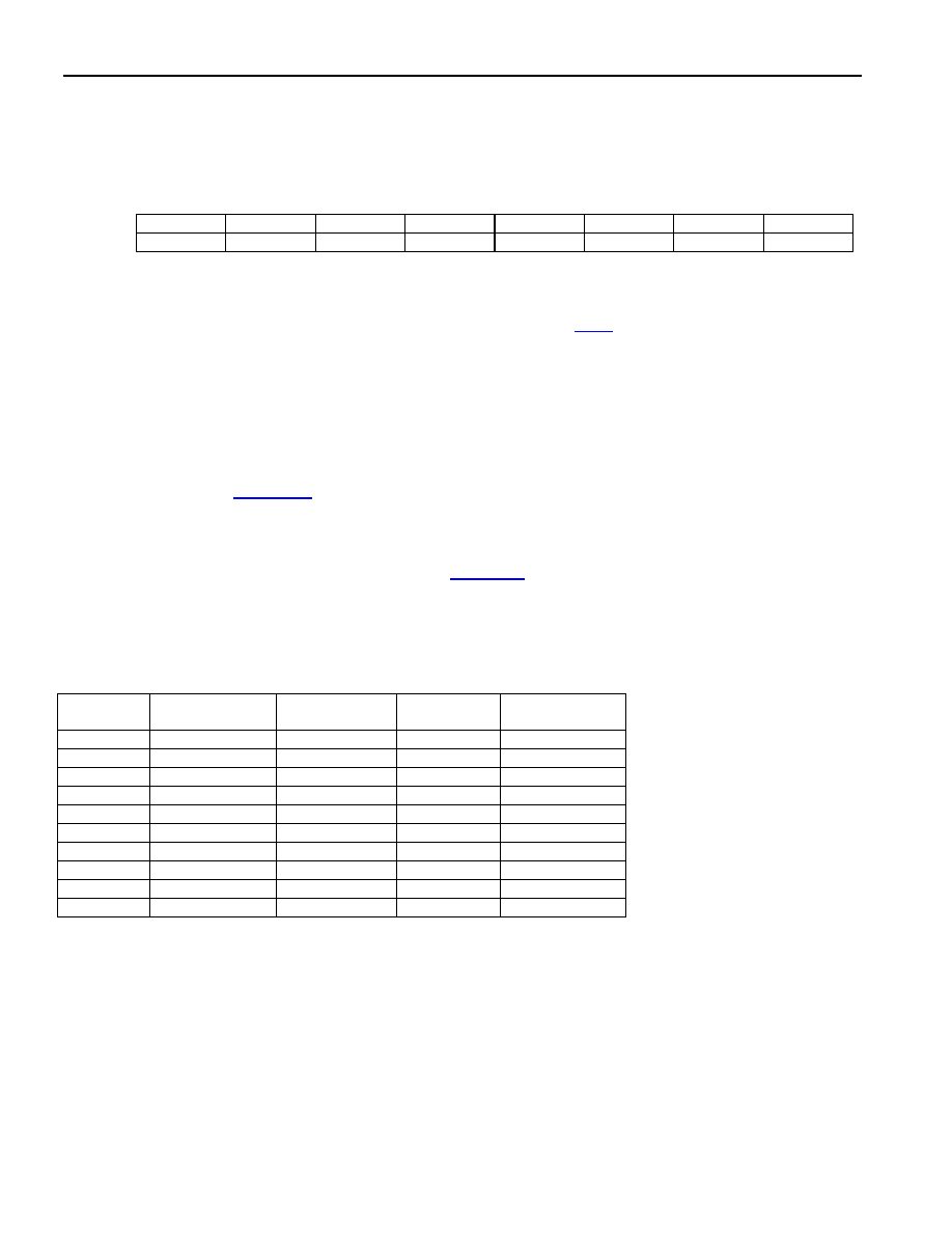
Register Name:
MC
Register Description:
Master Clock Select
Register Address:
06h
Bit #
7
6
5
4
3
2
1
0
Name
PCLKI1
PCLKI0
TECLKE
CLKAE
MPS1
MPS0
FREQS
PLLE
Default
0
Bits 7 and 6: PLL Clock Input [1:0] (PCLKI[1:0]). These bits select the input into to the PLL.
00: MCLK is used.
01: RCLK1 to 8 is used based on the selection in register CCR.
10: RCLK9 to 16 is used based on the selection in register CCR.
11: Reserved.
Bit 5: T1/E1 Clock Enable (TECLKE). When this bit is set the TECLK output is enabled. If not set TECLK will be
disabled and the TECLK output is a LOS output. TECLK requires PLLE to be set for correct functionality.
Bit 4: Clock A Enable (CLKAE). When this bit is set the CLKA output is enabled. If not set CLKA will be disabled
and the CLKA output is a LOS output. CLKA requires PLLE to be set for correct functionality.
Bits 3 and 2: Master Period Select [1:0] (MPS[1:0]). These bits MPS[1:0] selects the external MCLK frequency
for the DS26324. See Table 6-15 for details. This register when written to will also controller functionality of
Channels 9 to 16.
Bit 1: Frequency Select (FREQS). In conjunction with MPS[1:0] selects the external MCLK frequency for the
DS26324. If this bit is set the external Master clock can be 1.544MHz or multiple thereof. If not set the external
master clock can be 2.048MHz or multiple thereof. See Table 6-15 for details. This register when written to will also
controller functionality of Channels 9 to 16.
Bit 0: Phase Lock Loop Enable (PLLE). When this bit is set the phase lock loop is enabled. If not set MCLK will
be the applied input clock.
Table 6-15. DS26324 MCLK Selections
PLLE
MPS1, MPS0
MCLK,
MHz ±50ppm
FREQS
MODE
0
xx
1.544
x
T1
0
xx
2.048
x
E1
1
00
1.544
1
T1/J1 or E1
1
01
3.088
1
T1/J1 or E1
1
10
6.176
1
T1/J1 or E1
1
11
12.352
1
T1/J1 or E1
1
00
2.048
0
T1/J1 or E1
1
01
4.096
0
T1/J1 or E1
1
10
8.192
0
T1/J1 or E1
1
11
16.384
0
T1/J1 or E1
相关PDF资料 |
PDF描述 |
|---|---|
| VE-JWH-EZ-F1 | CONVERTER MOD DC/DC 52V 25W |
| GCC18DRES | CONN EDGECARD 36POS .100 EYELET |
| DS26334DK | KIT DESIGN FOR DS26334 |
| VE-JWH-EY-S | CONVERTER MOD DC/DC 52V 50W |
| GCC19DREN | CONN EDGECARD 38POS .100 EYELET |
相关代理商/技术参数 |
参数描述 |
|---|---|
| DS26324G | 功能描述:电信集成电路 3.3V E1/T1/J1 16Ch Short Haul Octal LIU RoHS:否 制造商:STMicroelectronics 类型:Telecom IC - Various 工作电源电压:4.75 V to 5.25 V 电源电流: 工作温度范围:- 40 C to + 85 C 安装风格:SMD/SMT 封装 / 箱体:PQFP-100 封装:Tray |
| DS26324G+ | 功能描述:电信集成电路 3.3V E1/T1/J1 16Ch Short Haul Octal LIU RoHS:否 制造商:STMicroelectronics 类型:Telecom IC - Various 工作电源电压:4.75 V to 5.25 V 电源电流: 工作温度范围:- 40 C to + 85 C 安装风格:SMD/SMT 封装 / 箱体:PQFP-100 封装:Tray |
| DS26324GA2 | 功能描述:电信集成电路 RoHS:否 制造商:STMicroelectronics 类型:Telecom IC - Various 工作电源电压:4.75 V to 5.25 V 电源电流: 工作温度范围:- 40 C to + 85 C 安装风格:SMD/SMT 封装 / 箱体:PQFP-100 封装:Tray |
| DS26324GA2+ | 功能描述:电信集成电路 RoHS:否 制造商:STMicroelectronics 类型:Telecom IC - Various 工作电源电压:4.75 V to 5.25 V 电源电流: 工作温度范围:- 40 C to + 85 C 安装风格:SMD/SMT 封装 / 箱体:PQFP-100 封装:Tray |
| DS26324GA2+W | 功能描述:电信集成电路 RoHS:否 制造商:STMicroelectronics 类型:Telecom IC - Various 工作电源电压:4.75 V to 5.25 V 电源电流: 工作温度范围:- 40 C to + 85 C 安装风格:SMD/SMT 封装 / 箱体:PQFP-100 封装:Tray |
发布紧急采购,3分钟左右您将得到回复。