- 您现在的位置:买卖IC网 > PDF目录1915 > DS32512N+ (Maxim Integrated Products)IC LIU DS3/E3/STS-1 12P 484-BGA PDF资料下载
参数资料
| 型号: | DS32512N+ |
| 厂商: | Maxim Integrated Products |
| 文件页数: | 74/130页 |
| 文件大小: | 0K |
| 描述: | IC LIU DS3/E3/STS-1 12P 484-BGA |
| 产品培训模块: | Lead (SnPb) Finish for COTS Obsolescence Mitigation Program |
| 标准包装: | 30 |
| 类型: | 线路接口装置(LIU) |
| 规程: | DS3 |
| 电源电压: | 3.135 V ~ 3.465 V |
| 安装类型: | 表面贴装 |
| 封装/外壳: | 484-BGA |
| 供应商设备封装: | 484-BGA(23x23) |
| 包装: | 管件 |
第1页第2页第3页第4页第5页第6页第7页第8页第9页第10页第11页第12页第13页第14页第15页第16页第17页第18页第19页第20页第21页第22页第23页第24页第25页第26页第27页第28页第29页第30页第31页第32页第33页第34页第35页第36页第37页第38页第39页第40页第41页第42页第43页第44页第45页第46页第47页第48页第49页第50页第51页第52页第53页第54页第55页第56页第57页第58页第59页第60页第61页第62页第63页第64页第65页第66页第67页第68页第69页第70页第71页第72页第73页当前第74页第75页第76页第77页第78页第79页第80页第81页第82页第83页第84页第85页第86页第87页第88页第89页第90页第91页第92页第93页第94页第95页第96页第97页第98页第99页第100页第101页第102页第103页第104页第105页第106页第107页第108页第109页第110页第111页第112页第113页第114页第115页第116页第117页第118页第119页第120页第121页第122页第123页第124页第125页第126页第127页第128页第129页第130页
DS32506/DS32508/DS32512
48 of 130
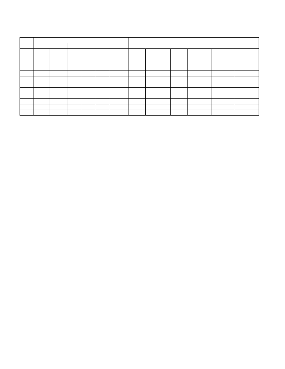
Table 8-16. Reset and Power-Down Sources
REGISTER BITS
PIN
GLOBAL.CR1
PORT.CR1
INTERNAL SIGNALS
RST RSTDP RST TPD RPD RSTDP
Global
Reset
Global
Data Path
Reset
Port
Reset
Tx Port
Power-
Down
Rx Port
Power-
Down
Port Data
Path
Reset
0
F0
F1
F0
F1
1
F1
F0
F1
1
0
1
0
1
0
1
0
1
F1
0
1
0
1
0
1
0
1
0
1
0
1
0
1
0
1
0
1
0
1
0
1
0
Register bit states: F0 = forced to 0, F1 = forced to 1, 0 = set to 0, 1 = set to 1
The reset signals in the device are asserted asynchronously and do not require a clock to put the logic into the
reset state. The control registers do not require a clock to come out of the reset state, but all other logic does
require a clock to come out of the reset state.
The port transmit power-down function (PORT.CR1:TPD) disables all the transmit clocks and powers down the
transmit LIU to minimize power consumption. The port receive power-down function (PORT.CR1:RPD) disables all
of the receive clocks and powers down the receive LIU to minimize power consumption. The one-second timer
circuit can be powered down by disabling its reference clock. The CLAD can be powered down by disabling it
(setting GLOBAL.CR2:CLAD[6:0] = 0). The global logic cannot be powered down.
After a global reset, all of the control and status registers in all ports are set to their default values and all the other
flip-flops are reset to their reset values. The global data path reset (GLOBAL.CR1:RSTDP), all the port data path
resets (PORT.CR1:RSTDP), and all the port power-down (PORT.CR1:TPD and RPD) bits are set after the global
reset. A valid initialization sequence is to clear the port power-down bits in the ports that are to be active, write to all
of the configuration registers to set them in the desired modes, then clear the GLOBAL.CR1:RSTDP and
PORT.CR1:RSTDP bits. This causes all the logic to start up in a predictable manner. The device can also be
writing to all of the configuration registers to set them in the desired modes, and then clearing all of the latched
status bits. This second initialization scheme can cause the device to operate unpredictably for a brief period of
time.
Some of the I/O pins are put into a known state at reset. At the global level, the microprocessor interface output
and I/O pins (D[15:0]) are forced into the high impedance state when the RST pin is active, but not when the
GLOBAL.CR1:RST bit is active. The CLAD clock pins CLKA, CLKB, and CLKC are forced to be the LIU reference
clock inputs. The general-purpose I/O pins (GPIOAn and GPIOBn) are forced to be inputs until after the RST pin is
deasserted. At the port level, the LIU transmitter outputs TXP and TXN are forced into a high-impedance state.
Note:
Setting any of the reset (RST), data path reset (RSTDP), or power-down (TPD, RPD) bits for less than 100
ns may result in the associated circuits coming up in a random state. When a power-down bit is cleared, it takes
approximately 1ms for all of the associated circuits to power-up.
相关PDF资料 |
PDF描述 |
|---|---|
| DS3254N+ | IC LIU DS3/E3/STS-1 144-CSBGA |
| DS33M33N+ | IC MAPPER ETHERNET 256CSBGA |
| DS33R11+CJ2 | IC ETH TXRX T1/E1/J1 256-BGA |
| DS33R41+ | IC TXRX ETHERNET MAP 400-BGA |
| DS33W11DK+ | IC MAPPING ETHERNET 256-CSBGA |
相关代理商/技术参数 |
参数描述 |
|---|---|
| DS32512N# | 功能描述:网络控制器与处理器 IC 12-Port DS3/E3/STS-1 Line Interface Unit RoHS:否 制造商:Micrel 产品:Controller Area Network (CAN) 收发器数量: 数据速率: 电源电流(最大值):595 mA 最大工作温度:+ 85 C 安装风格:SMD/SMT 封装 / 箱体:PBGA-400 封装:Tray |
| DS32512N+ | 功能描述:网络控制器与处理器 IC 12-Port DS3/E3/STS-1 Line Interface Unit RoHS:否 制造商:Micrel 产品:Controller Area Network (CAN) 收发器数量: 数据速率: 电源电流(最大值):595 mA 最大工作温度:+ 85 C 安装风格:SMD/SMT 封装 / 箱体:PBGA-400 封装:Tray |
| DS32512NA2 | 制造商:Maxim Integrated Products 功能描述:DS32512 X12 DS3/E3 LIU REVA2 IND - Rail/Tube |
| DS32512NW | 功能描述:网络控制器与处理器 IC RoHS:否 制造商:Micrel 产品:Controller Area Network (CAN) 收发器数量: 数据速率: 电源电流(最大值):595 mA 最大工作温度:+ 85 C 安装风格:SMD/SMT 封装 / 箱体:PBGA-400 封装:Tray |
| DS32512W | 功能描述:网络控制器与处理器 IC RoHS:否 制造商:Micrel 产品:Controller Area Network (CAN) 收发器数量: 数据速率: 电源电流(最大值):595 mA 最大工作温度:+ 85 C 安装风格:SMD/SMT 封装 / 箱体:PBGA-400 封装:Tray |
发布紧急采购,3分钟左右您将得到回复。