- 您现在的位置:买卖IC网 > PDF目录9751 > DS3253N+ (Maxim Integrated Products)IC LIU DS3/E3/STS-1 144-CSBGA PDF资料下载
参数资料
| 型号: | DS3253N+ |
| 厂商: | Maxim Integrated Products |
| 文件页数: | 20/71页 |
| 文件大小: | 0K |
| 描述: | IC LIU DS3/E3/STS-1 144-CSBGA |
| 产品培训模块: | Lead (SnPb) Finish for COTS Obsolescence Mitigation Program |
| 标准包装: | 160 |
| 类型: | 线路接口装置(LIU) |
| 驱动器/接收器数: | 3/3 |
| 规程: | IEEE 1149.1 |
| 电源电压: | 3.135 V ~ 3.465 V |
| 安装类型: | 表面贴装 |
| 封装/外壳: | 144-BGA,CSPBGA |
| 供应商设备封装: | 144-TECSBGA(13x13) |
| 包装: | 托盘 |
第1页第2页第3页第4页第5页第6页第7页第8页第9页第10页第11页第12页第13页第14页第15页第16页第17页第18页第19页当前第20页第21页第22页第23页第24页第25页第26页第27页第28页第29页第30页第31页第32页第33页第34页第35页第36页第37页第38页第39页第40页第41页第42页第43页第44页第45页第46页第47页第48页第49页第50页第51页第52页第53页第54页第55页第56页第57页第58页第59页第60页第61页第62页第63页第64页第65页第66页第67页第68页第69页第70页第71页
DS3251/DS3252/DS3253/DS3254
27 of 71
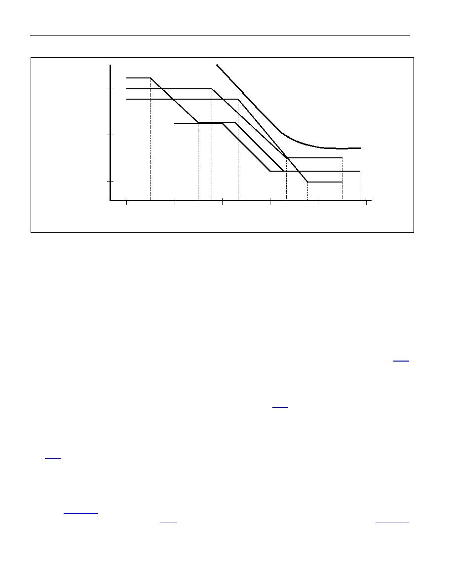
Figure 8-1. Receiver Jitter Tolerance
9. TRANSMITTER
9.1 Transmit Clock
The clock applied at the TCLK input clocks in data on the TPOS/TDAT and TNEG pins. If the jitter attenuator is not
enabled in the transmit path, the signal on TCLK is the transmit line clock and must be transmission quality (i.e.,
±20ppm frequency accuracy and low jitter). If the jitter attenuator is enabled in the transmit path, the signal on
TCLK can be jittery and/or periodically gapped, but must still have an average frequency within
±20ppm of the
nominal line rate. When enabled in the transmit path, the jitter attenuator generates the transmit line clock from the
appropriate master clock.
The polarity of TCLK can be inverted to support glueless interfacing to a variety of neighboring components.
Normally data is sampled on the TPOS/TDAT and TNEG pins on the rising edge of TCLK. To sample data on the
falling edge of TCLK, pull the TCINV pin high (hardware mode) or set the TCINV configuration bit in the TCR
register (CPU bus mode).
9.2 Framer Interface Format and the B3ZS/HDB3 Encoder
Data to be transmitted can be input in either binary or bipolar format. To select the binary interface format, pull the
TBIN pin high (hardware mode) or set the TBIN configuration bit in the TCR register (CPU bus mode). In binary
format, the B3ZS/HBD3 encoder is enabled, and the data to be transmitted is sampled on the TDAT pin. The
TNEG pin is ignored in binary interface mode and should be wired low. In DS3 and STS-1 modes, the B3ZS/HDB3
encoder operates in the B3ZS mode. In E3 mode the encoder operates in HDB3 mode.
To select the bipolar interface format, pull the TBIN pin low (hardware mode) or clear the TBIN configuration bit in
the TCR register (CPU bus mode). In bipolar format, the B3ZS/HDB3 encoder is disabled and the data to be
transmitted is sampled on the TPOS and TNEG pins. Positive-polarity pulses are indicated by TPOS = 1, while
negative-polarity pulses are indicated by TNEG = 1.
9.3 Pattern Generation
The transmitter can generate several patterns internally, including unframed all ones (E3 AIS), 100100…, and DS3
AIS. See Figure 9-2 for the structure of the DS3 AIS signal. The TDSA and TDSB input pins (hardware mode) or
the TDSA and TDSB control bits in the GCR register (CPU bus mode) are used to select these patterns. Table 6-G
indicates the possible selections.
10
100
1k
10k
100k
1M
60k
22.3k
2.3k
669
0.1
1.0
10
300k
800k
300
30
0.1
0.15
0.3
10
5
1.5
E3 G.823
DS3 GR-499 Cat II
DS3 GR-499 Cat I
DS325x JITTER TOLERANCE
15
STS-1 GR253
FREQUENCY (Hz)
JITTER
TOLERANCE
(UI
P-
P
)
相关PDF资料 |
PDF描述 |
|---|---|
| DS26528GN+ | IC TXRX T1/E1/J1 OCT 256-CSBGA |
| MAX1076CTC+ | IC ADC 10BIT 1.8MSPS 12-TQFN |
| MC100EP17DWG | IC RCVR/DRV ECL QUAD DIFF 20SOIC |
| DS26324GN+ | IC LIU 16CH T1/E1/J1 256CSBGA |
| MC100EP116MNG | IC LINE RCVR/DRVR HEX DIFF 32QFN |
相关代理商/技术参数 |
参数描述 |
|---|---|
| DS3253N# | 功能描述:网络控制器与处理器 IC Triple DS3/E3/STS-1 Line Interface Unit RoHS:否 制造商:Micrel 产品:Controller Area Network (CAN) 收发器数量: 数据速率: 电源电流(最大值):595 mA 最大工作温度:+ 85 C 安装风格:SMD/SMT 封装 / 箱体:PBGA-400 封装:Tray |
| DS3253N+ | 功能描述:网络控制器与处理器 IC Triple DS3/E3/STS-1 Line Interface Unit RoHS:否 制造商:Micrel 产品:Controller Area Network (CAN) 收发器数量: 数据速率: 电源电流(最大值):595 mA 最大工作温度:+ 85 C 安装风格:SMD/SMT 封装 / 箱体:PBGA-400 封装:Tray |
| DS3253NA3 | 制造商:Maxim Integrated Products 功能描述:DS3253 REV A3 - Rail/Tube |
| DS3254 | 功能描述:网络控制器与处理器 IC Quad DS3/E3/STS-1 Line Interface Unit RoHS:否 制造商:Micrel 产品:Controller Area Network (CAN) 收发器数量: 数据速率: 电源电流(最大值):595 mA 最大工作温度:+ 85 C 安装风格:SMD/SMT 封装 / 箱体:PBGA-400 封装:Tray |
| DS3254+ | 功能描述:网络控制器与处理器 IC Quad DS3/E3/STS-1 Line Interface Unit RoHS:否 制造商:Micrel 产品:Controller Area Network (CAN) 收发器数量: 数据速率: 电源电流(最大值):595 mA 最大工作温度:+ 85 C 安装风格:SMD/SMT 封装 / 箱体:PBGA-400 封装:Tray |
发布紧急采购,3分钟左右您将得到回复。