- 您现在的位置:买卖IC网 > PDF目录1994 > DS32C35-33#T&R (Maxim Integrated Products)IC RTC ACCURATE I2C 3.3V 20-SOIC PDF资料下载
参数资料
| 型号: | DS32C35-33#T&R |
| 厂商: | Maxim Integrated Products |
| 文件页数: | 18/22页 |
| 文件大小: | 0K |
| 描述: | IC RTC ACCURATE I2C 3.3V 20-SOIC |
| 产品变化通告: | Product Discontinuation 28/Nov/2011 |
| 标准包装: | 1,000 |
| 类型: | 时钟/日历 |
| 特点: | 警报器,FRAM,闰年,方波输出,TCXO/晶体 |
| 存储容量: | 8KB |
| 时间格式: | HH:MM:SS(12/24 小时) |
| 数据格式: | YY-MM-DD-dd |
| 接口: | I²C,2 线串口 |
| 电源电压: | 2.7 V ~ 3.63 V |
| 电压 - 电源,电池: | 2.3 V ~ 3.6 V |
| 工作温度: | 0°C ~ 70°C |
| 安装类型: | 表面贴装 |
| 封装/外壳: | 20-SOIC(0.295",7.50mm 宽) |
| 供应商设备封装: | 20-SOIC W |
| 包装: | 带卷 (TR) |
DS32B35/DS32C35
Accurate I2C RTC with Integrated
TCXO/Crystal/FRAM
_____________________________________________________________________
5
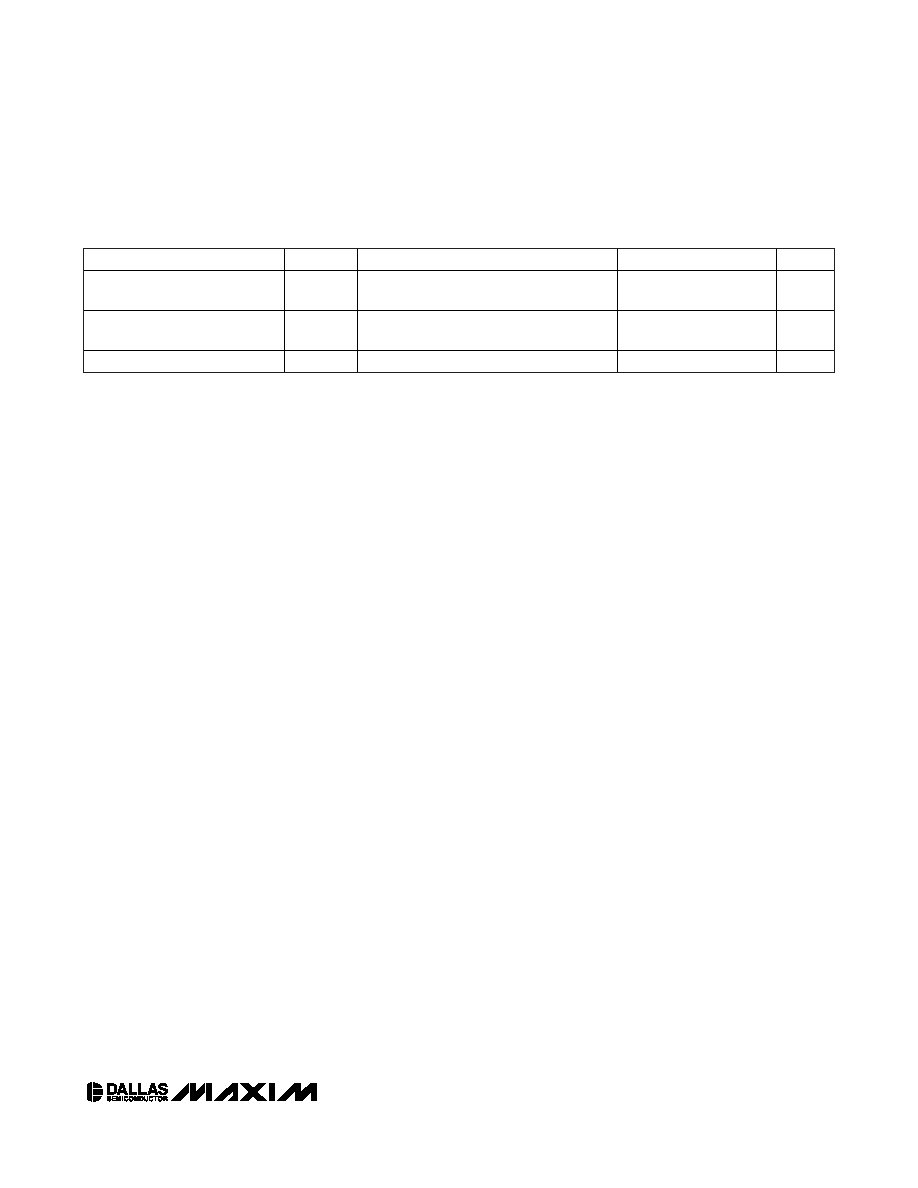
POWER-SWITCH CHARACTERISTICS
(TA = -40°C to +85°C, Note 2, see the Power-Switch Timing diagram.)
PARAMETER
SYMBOL
CONDITIONS
MIN
TYP
MAX
UNITS
VCC Fall Time; VPF(MAX) to
VPF(MIN)
tVCCF
300
μs
VCC Rise Time; VPF(MIN) to
VPF(MAX)
tVCCR
0
μs
Recovery at Power-Up
tREC
(Note 14)
300
ms
Note 2:
Limits at -40°C are guaranteed by design and not production tested.
Note 3:
All voltages are referenced to ground.
Note 4:
To minimize current drain on VBAT when the internal supply is switched to VBAT, the VIH minimum must be higher than
VBAT - 0.6V. Otherwise, there is significant current drain due to the input stage at the SCL and SDA pins.
Note 5:
The pullup resistor voltage on the 32kHz and INT/SQW pins can be up to 5.5V maximum regardless of the voltage on VCC.
Note 6:
Current is the averaged input current, which includes the temperature conversion current.
Note 7:
The RST pin has an internal 50k
Ω (nominal) pullup resistor to VCC.
Note 8:
After this period, the first clock pulse is generated.
Note 9:
A device must internally provide a hold time of at least 300ns for the SDA signal (referred to as the VIH(MIN) of the SCL sig-
nal) to bridge the undefined region of the falling edge of SCL.
Note 10: The maximum tHD:DAT needs only to be met if the device does not stretch the low period (tLOW) of the SCL signal.
Note 11: A fast-mode device can be used in a standard-mode system, but the requirement tSU:DAT
≥ 250ns must then be met. This
is automatically the case if the device does not stretch the low period of the SCL signal. If such a device does stretch the
low period of the SCL signal, it must output the next data bit to the SDA line tR(MAX) + tSU:DAT = 1000 + 250 = 1250ns
before the SCL line is released.
Note 12: CB—total capacitance of one bus line in pF.
Note 13: The parameter tOSF is the period of time the oscillator must be stopped for the OSF flag to be set over the voltage range of
0.0V
≤ VCC ≤ VCC(MAX) and 2.0V ≤ VBAT ≤ 3.6V.
Note 14: This delay applies only if the oscillator is enabled and running. If the EOSC bit is a 1, tREC is bypassed and RST immedi-
ately goes high. The state of RST does not affect the I2C interface, RTC, TCXO, or FRAM operation.
WARNING: Negative undershoots below -0.3V while the part is in battery-backed mode may cause loss of data.
相关PDF资料 |
PDF描述 |
|---|---|
| DS3911T+ | IC DAC 10BIT I2C QUAD 14TDFN |
| DS4000KI/WBGA | IC OSC TCXO 19.44MHZ 24-BGA |
| DS4026S+WCN | IC OSC TCXO 25MHZ 16-SOIC |
| DS4100HW+ | IC OSC CLOCK 100MHZ 10LCCC |
| DS4266P+ | IC OSC CLOCK 266MHZ 10-LCCC |
相关代理商/技术参数 |
参数描述 |
|---|---|
| DS32EL0124 | 制造商:NSC 制造商全称:National Semiconductor 功能描述:125 MHz . 312.5 MHz Deserializer with DDR LVDS Parallel Interface |
| DS32EL0124_0807 | 制造商:NSC 制造商全称:National Semiconductor 功能描述:125 MHz . 312.5 MHz Deserializer with DDR LVDS Parallel Interface |
| DS32EL0124_09 | 制造商:NSC 制造商全称:National Semiconductor 功能描述:125 MHz- 312.5 MHz FPGA-Link Deserializer with DDR LVDS Parallel Interface |
| DS32EL0124SQ | 制造商:NSC 制造商全称:National Semiconductor 功能描述:125 MHz- 312.5 MHz FPGA-Link Deserializer with DDR LVDS Parallel Interface |
| DS32EL0124SQ/NOPB | 功能描述:LVDS 接口集成电路 RoHS:否 制造商:Texas Instruments 激励器数量:4 接收机数量:4 数据速率:155.5 Mbps 工作电源电压:5 V 最大功率耗散:1025 mW 最大工作温度:+ 85 C 封装 / 箱体:SOIC-16 Narrow 封装:Reel |
发布紧急采购,3分钟左右您将得到回复。