- 您现在的位置:买卖IC网 > PDF目录16258 > DS33X162DK (Maxim Integrated Products)KIT DEMO FOR DS33X162+ PDF资料下载
参数资料
| 型号: | DS33X162DK |
| 厂商: | Maxim Integrated Products |
| 文件页数: | 135/375页 |
| 文件大小: | 0K |
| 描述: | KIT DEMO FOR DS33X162+ |
| 产品培训模块: | Lead (SnPb) Finish for COTS Obsolescence Mitigation Program |
| 标准包装: | 1 |
| 主要目的: | 接口,以太网 |
| 已用 IC / 零件: | DS33X162+ |
第1页第2页第3页第4页第5页第6页第7页第8页第9页第10页第11页第12页第13页第14页第15页第16页第17页第18页第19页第20页第21页第22页第23页第24页第25页第26页第27页第28页第29页第30页第31页第32页第33页第34页第35页第36页第37页第38页第39页第40页第41页第42页第43页第44页第45页第46页第47页第48页第49页第50页第51页第52页第53页第54页第55页第56页第57页第58页第59页第60页第61页第62页第63页第64页第65页第66页第67页第68页第69页第70页第71页第72页第73页第74页第75页第76页第77页第78页第79页第80页第81页第82页第83页第84页第85页第86页第87页第88页第89页第90页第91页第92页第93页第94页第95页第96页第97页第98页第99页第100页第101页第102页第103页第104页第105页第106页第107页第108页第109页第110页第111页第112页第113页第114页第115页第116页第117页第118页第119页第120页第121页第122页第123页第124页第125页第126页第127页第128页第129页第130页第131页第132页第133页第134页当前第135页第136页第137页第138页第139页第140页第141页第142页第143页第144页第145页第146页第147页第148页第149页第150页第151页第152页第153页第154页第155页第156页第157页第158页第159页第160页第161页第162页第163页第164页第165页第166页第167页第168页第169页第170页第171页第172页第173页第174页第175页第176页第177页第178页第179页第180页第181页第182页第183页第184页第185页第186页第187页第188页第189页第190页第191页第192页第193页第194页第195页第196页第197页第198页第199页第200页第201页第202页第203页第204页第205页第206页第207页第208页第209页第210页第211页第212页第213页第214页第215页第216页第217页第218页第219页第220页第221页第222页第223页第224页第225页第226页第227页第228页第229页第230页第231页第232页第233页第234页第235页第236页第237页第238页第239页第240页第241页第242页第243页第244页第245页第246页第247页第248页第249页第250页第251页第252页第253页第254页第255页第256页第257页第258页第259页第260页第261页第262页第263页第264页第265页第266页第267页第268页第269页第270页第271页第272页第273页第274页第275页第276页第277页第278页第279页第280页第281页第282页第283页第284页第285页第286页第287页第288页第289页第290页第291页第292页第293页第294页第295页第296页第297页第298页第299页第300页第301页第302页第303页第304页第305页第306页第307页第308页第309页第310页第311页第312页第313页第314页第315页第316页第317页第318页第319页第320页第321页第322页第323页第324页第325页第326页第327页第328页第329页第330页第331页第332页第333页第334页第335页第336页第337页第338页第339页第340页第341页第342页第343页第344页第345页第346页第347页第348页第349页第350页第351页第352页第353页第354页第355页第356页第357页第358页第359页第360页第361页第362页第363页第364页第365页第366页第367页第368页第369页第370页第371页第372页第373页第374页第375页
________________________________________________ DS33X162/X161/X82/X81/X42/X41/X11/W41/W11
Rev: 063008
22 of 375
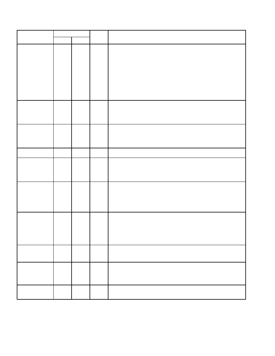
PACKAGE PINS
NAME
256
144
TYPE
FUNCTION
D5/
SPI_SWAP
L8
J5
IOz
Data Bit 5. Bi-directional data bit 5 of the microprocessor interface. Not
driven when
CS=1 or RST=0.
SPI_SWAP (SPI_SEL=1). Controls the address and data bit order of the
SPI interface. The R/W and B bit positions do not change.
0 = LSB is transmitted and received first. The resulting bit order is:
R/W, A7, A8, A9, A10, A11, A12, A13,
A0, A1, A2, A3, A4, A5, A6, Burst,
D0, D1, D2, D3, D4, D5, D6, D7...
1 = MSB is transmitted and received first. The resulting bit order is:
R/W, A13, A12, A11, A10, A9, A8, A7,
A6, A5, A4, A3, A2, A1, A0, Burst,
D7, D6, D5, D4, D3, D2, D1, D0…
D6/
SPI_CPHA
K9
K5
IOz
Data Bit 6. Bi-directional data bit 6 of the microprocessor interface. Not
driven when
CS=1 or RST=0.
SPI_CPHA (SPI_SEL=1). When in SPI mode, setting this bit to 1 inverts
the phase of the clock signal on SPICK. See Section 2.10 for detailed
timing and functionality information. Default setting is low.
D7/
SPI_CPOL
M9
L5
IOz
Data Bit 7. Bi-directional data bit 7 of the microprocessor interface. Not
driven when
CS=1 or RST=0.
SPI_CPOL (SPI_SEL=1). When in SPI mode, setting this bit to 1 inverts
the clock signal on SPICK. See Section 2.10 for detailed timing and
functionality information. Default setting is low.
CS
J8
J3
I
Chip Select. This pin must be taken low for read/write operations. When
CS is high, the RD/DS and WR signals are ignored.
RD/DS
J9
—
I
Read Data Strobe (Intel Mode). The device drives the data bus with the
contents of the addressed register while
RD and CS are both low.
Data Strobe (Motorola Mode). Used to latch data through the
microprocessor interface.
DS must be low during read and write
operations.
WR/RW
J10
—
I
Write (Intel Mode). The device captures the contents of the data bus on
the rising edge of
WR and writes them to the addressed register location.
CS must be held low during write operations.
Read Write (Motorola Mode). Used to indicate read or write operation.
R
W must be set high for a register read cycle and low for a register write
cycle.
ALE
J7
—
I
Address Latch Enable. This signal is used to internally latch an address,
allowing multiplexing of the parallel interface address and data lines.
When ALE is high, the values of the A[10:0] pins are used for read/write
operations. On the falling edge of ALE, the values of the A[10:0] pins are
latched internally, and the latched value is used for read/write operations
until the next rising edge of ALE. ALE should be tied high for non-
multiplexed address systems.
MODE
J12
—
I
Mode. Selects
RD/WR or DS strobe mode.
0 = Read/Write Strobe Mode
1 = Data Strobe Mode
INT
J11
G5
Oz
Interrupt Output. Outputs a logic zero when an unmasked interrupt event
is detected.
INT is de-asserted when all interrupts have been
acknowledged and serviced. Active low. Inactive state is configured with
the GL.CR2.INTM bit.
SPI_SEL
J16
—
I
Parallel/SPI Interface Select
0 = Parallel Interface
1 = SPI Interface Selected
相关PDF资料 |
PDF描述 |
|---|---|
| ECO-S2EB102DA | CAP ALUM 1000UF 250V 20% SNAP |
| GCA32DRMD-S288 | CONN EDGECARD 64POS .125 EXTEND |
| RBC10DCAI | CONN EDGECARD 20POS R/A .100 SLD |
| ECO-S1EA333EA | CAP ALUM 33000UF 25V 20% SNAP |
| DS33X11DK | KIT DEMO FOR DS33X11+ |
相关代理商/技术参数 |
参数描述 |
|---|---|
| DS33X41 | 功能描述:网络控制器与处理器 IC Ethernet Over PDH Mapping Devices RoHS:否 制造商:Micrel 产品:Controller Area Network (CAN) 收发器数量: 数据速率: 电源电流(最大值):595 mA 最大工作温度:+ 85 C 安装风格:SMD/SMT 封装 / 箱体:PBGA-400 封装:Tray |
| DS33X41+ | 功能描述:网络控制器与处理器 IC Ethernet Over PDH Mapping Devices RoHS:否 制造商:Micrel 产品:Controller Area Network (CAN) 收发器数量: 数据速率: 电源电流(最大值):595 mA 最大工作温度:+ 85 C 安装风格:SMD/SMT 封装 / 箱体:PBGA-400 封装:Tray |
| DS33X42+ | 功能描述:网络控制器与处理器 IC Ethernet Over PDH Mapping Devices RoHS:否 制造商:Micrel 产品:Controller Area Network (CAN) 收发器数量: 数据速率: 电源电流(最大值):595 mA 最大工作温度:+ 85 C 安装风格:SMD/SMT 封装 / 箱体:PBGA-400 封装:Tray |
| DS33X42DK | 功能描述:以太网开发工具 DS33X42 Dev Kit RoHS:否 制造商:Micrel 产品:Evaluation Boards 类型:Ethernet Transceivers 工具用于评估:KSZ8873RLL 接口类型:RMII 工作电源电压: |
| DS33X81+ | 功能描述:网络控制器与处理器 IC Ethernet Over PDH Mapping Devices RoHS:否 制造商:Micrel 产品:Controller Area Network (CAN) 收发器数量: 数据速率: 电源电流(最大值):595 mA 最大工作温度:+ 85 C 安装风格:SMD/SMT 封装 / 箱体:PBGA-400 封装:Tray |
发布紧急采购,3分钟左右您将得到回复。