- 您现在的位置:买卖IC网 > PDF目录16258 > DS33X162DK (Maxim Integrated Products)KIT DEMO FOR DS33X162+ PDF资料下载
参数资料
| 型号: | DS33X162DK |
| 厂商: | Maxim Integrated Products |
| 文件页数: | 179/375页 |
| 文件大小: | 0K |
| 描述: | KIT DEMO FOR DS33X162+ |
| 产品培训模块: | Lead (SnPb) Finish for COTS Obsolescence Mitigation Program |
| 标准包装: | 1 |
| 主要目的: | 接口,以太网 |
| 已用 IC / 零件: | DS33X162+ |
第1页第2页第3页第4页第5页第6页第7页第8页第9页第10页第11页第12页第13页第14页第15页第16页第17页第18页第19页第20页第21页第22页第23页第24页第25页第26页第27页第28页第29页第30页第31页第32页第33页第34页第35页第36页第37页第38页第39页第40页第41页第42页第43页第44页第45页第46页第47页第48页第49页第50页第51页第52页第53页第54页第55页第56页第57页第58页第59页第60页第61页第62页第63页第64页第65页第66页第67页第68页第69页第70页第71页第72页第73页第74页第75页第76页第77页第78页第79页第80页第81页第82页第83页第84页第85页第86页第87页第88页第89页第90页第91页第92页第93页第94页第95页第96页第97页第98页第99页第100页第101页第102页第103页第104页第105页第106页第107页第108页第109页第110页第111页第112页第113页第114页第115页第116页第117页第118页第119页第120页第121页第122页第123页第124页第125页第126页第127页第128页第129页第130页第131页第132页第133页第134页第135页第136页第137页第138页第139页第140页第141页第142页第143页第144页第145页第146页第147页第148页第149页第150页第151页第152页第153页第154页第155页第156页第157页第158页第159页第160页第161页第162页第163页第164页第165页第166页第167页第168页第169页第170页第171页第172页第173页第174页第175页第176页第177页第178页当前第179页第180页第181页第182页第183页第184页第185页第186页第187页第188页第189页第190页第191页第192页第193页第194页第195页第196页第197页第198页第199页第200页第201页第202页第203页第204页第205页第206页第207页第208页第209页第210页第211页第212页第213页第214页第215页第216页第217页第218页第219页第220页第221页第222页第223页第224页第225页第226页第227页第228页第229页第230页第231页第232页第233页第234页第235页第236页第237页第238页第239页第240页第241页第242页第243页第244页第245页第246页第247页第248页第249页第250页第251页第252页第253页第254页第255页第256页第257页第258页第259页第260页第261页第262页第263页第264页第265页第266页第267页第268页第269页第270页第271页第272页第273页第274页第275页第276页第277页第278页第279页第280页第281页第282页第283页第284页第285页第286页第287页第288页第289页第290页第291页第292页第293页第294页第295页第296页第297页第298页第299页第300页第301页第302页第303页第304页第305页第306页第307页第308页第309页第310页第311页第312页第313页第314页第315页第316页第317页第318页第319页第320页第321页第322页第323页第324页第325页第326页第327页第328页第329页第330页第331页第332页第333页第334页第335页第336页第337页第338页第339页第340页第341页第342页第343页第344页第345页第346页第347页第348页第349页第350页第351页第352页第353页第354页第355页第356页第357页第358页第359页第360页第361页第362页第363页第364页第365页第366页第367页第368页第369页第370页第371页第372页第373页第374页第375页
________________________________________________ DS33X162/X161/X82/X81/X42/X41/X11/W41/W11
Rev: 063008
26 of 375
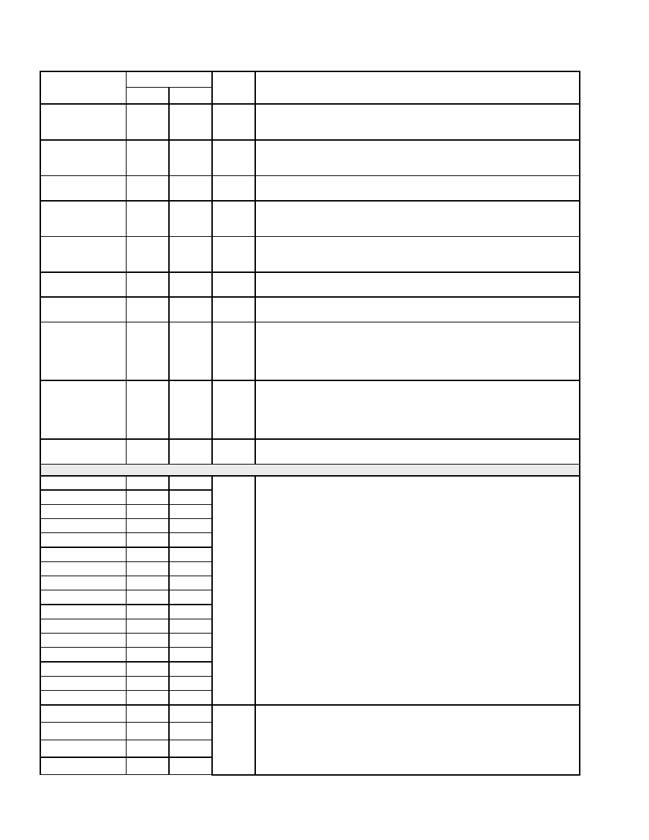
PACKAGE PINS
NAME
256
144
TYPE
FUNCTION
SRAS
A6
B5
O
SDRAM Row Address Strobe. Active-low output, used to latch the row
address on rising edge of SD_CLK. It is used with commands for Bank
Activate, Precharge, and Mode Register Write.
SCAS
B7
D5
O
SDRAM Column Address Strobe. Active low output, used to latch the
column address on the rising edge of SD_CLK. It is used with commands
for Bank Activate, Precharge, and Mode Register Write.
SWE
A7
C5
O
SDRAM Write Enable. This active low output enables write operation and
auto precharge.
SD_UDM
D7
E7
O
SDRAM Upper Data Mask. SD_UDM is an active high output mask
signal for write data. SD_UDM is updated on both edges of SD_UDQS.
SD_UDM corresponds to data on SDATA15-SDATA8.
SD_LDM
D13
E6
O
SDRAM Lower Data Mask. SD_LDM is an active high output mask signal
for write data. SD_LDM is updated on both edges of SD_LDQS. SD_LDM
corresponds to data on SDATA7-SDATA0.
SD_LDQS
C13
E8
IOz
Lower Data Strobe. Output with write data, input with read data.
SD_LDQS corresponds to data on SDATA7-SDATA0.
SD_UDQS
D8
D7
IOz
Upper Data Strobe. Output with write data, input with read data.
SD_UDQS corresponds to data on SDATA15-SDATA8.
SD_CLK
A8
O
SDRAM Clock. SD_CLK and
SD_CLK are differential clock outputs. All
address and control input signals are sampled on the crossing of the
positive edge of SD_CLK and negative edge of SD_CLK. Output (write)
data is referenced to the crossings of SD_CLK and
SD_CLK (both
directions of crossing).
SD_CLK
A9
A7
O
SDRAM Clock (Inverted). SD_CLK and
SD_CLK are differential clock
outputs. All address and control input signals are sampled on the crossing
of the positive edge of SD_CLK and negative edge of SD_CLK. Output
(write) data is referenced to the crossings of SD_CLK and
SD_CLK (both
directions of crossing).
SD_CLKEN
C4
E5
O
SDRAM Clock Enable. Active High. SD_CLKEN must be active
throughout DDR SDRAM READ and WRITE accesses.
SERIAL INTERFACE IO PINS
TDATA1
T6
L3
TDATA2
T7
—
TDATA3
P6
—
TDATA4
N9
—
TDATA5
M5
—
TDATA6
N6
—
TDATA7
N7
—
TDATA8
R9
—
TDATA9
N10
—
TDATA10
R11
—
TDATA11
N11
—
TDATA12
R12
—
TDATA13
P14
—
TDATA14
P12
—
TDATA15
N12
—
TDATA16
P11
—
O
Transmit Serial Data Output. Output on the rising edge of TCLK. The
maximum data rate is 52Mbps.
Not all serial port signals are available on all products in the device family.
Unused output pins should not be connected.
DS33X41/X42/W41/W11: TDATA5 – TDATA16 not used.
DS33X81/X82: TDATA9 – TDATA16 not used.
TCLK1/TMCLK1
R5
M3
TCLK2
P5
—
TCLK3
R8
—
TCLK4
P9
—
I
Serial Interface Transmit Clock Input (TCLK[1:8]).The clock reference
for TDATA, which is output on the rising edge of the clock. TCLK supports
gapped clocking, up to a maximum frequency of 52MHz.
Note that TCLK1 is also TMCLK1, TCLK5 is also TMCLK2. TMCLK3
and TMCLK4 are stand-alone pins.
相关PDF资料 |
PDF描述 |
|---|---|
| ECO-S2EB102DA | CAP ALUM 1000UF 250V 20% SNAP |
| GCA32DRMD-S288 | CONN EDGECARD 64POS .125 EXTEND |
| RBC10DCAI | CONN EDGECARD 20POS R/A .100 SLD |
| ECO-S1EA333EA | CAP ALUM 33000UF 25V 20% SNAP |
| DS33X11DK | KIT DEMO FOR DS33X11+ |
相关代理商/技术参数 |
参数描述 |
|---|---|
| DS33X41 | 功能描述:网络控制器与处理器 IC Ethernet Over PDH Mapping Devices RoHS:否 制造商:Micrel 产品:Controller Area Network (CAN) 收发器数量: 数据速率: 电源电流(最大值):595 mA 最大工作温度:+ 85 C 安装风格:SMD/SMT 封装 / 箱体:PBGA-400 封装:Tray |
| DS33X41+ | 功能描述:网络控制器与处理器 IC Ethernet Over PDH Mapping Devices RoHS:否 制造商:Micrel 产品:Controller Area Network (CAN) 收发器数量: 数据速率: 电源电流(最大值):595 mA 最大工作温度:+ 85 C 安装风格:SMD/SMT 封装 / 箱体:PBGA-400 封装:Tray |
| DS33X42+ | 功能描述:网络控制器与处理器 IC Ethernet Over PDH Mapping Devices RoHS:否 制造商:Micrel 产品:Controller Area Network (CAN) 收发器数量: 数据速率: 电源电流(最大值):595 mA 最大工作温度:+ 85 C 安装风格:SMD/SMT 封装 / 箱体:PBGA-400 封装:Tray |
| DS33X42DK | 功能描述:以太网开发工具 DS33X42 Dev Kit RoHS:否 制造商:Micrel 产品:Evaluation Boards 类型:Ethernet Transceivers 工具用于评估:KSZ8873RLL 接口类型:RMII 工作电源电压: |
| DS33X81+ | 功能描述:网络控制器与处理器 IC Ethernet Over PDH Mapping Devices RoHS:否 制造商:Micrel 产品:Controller Area Network (CAN) 收发器数量: 数据速率: 电源电流(最大值):595 mA 最大工作温度:+ 85 C 安装风格:SMD/SMT 封装 / 箱体:PBGA-400 封装:Tray |
发布紧急采购,3分钟左右您将得到回复。