- 您现在的位置:买卖IC网 > PDF目录11038 > DS72612RB120FPV (Renesas Electronics America)IC SUPERH MPU ROMLESS 176LQFP PDF资料下载
参数资料
| 型号: | DS72612RB120FPV |
| 厂商: | Renesas Electronics America |
| 文件页数: | 5/226页 |
| 文件大小: | 0K |
| 描述: | IC SUPERH MPU ROMLESS 176LQFP |
| 产品培训模块: | CAN Basics Part-1 CAN Basics Part-2 Electromagnetic Noise Reduction Techniques Part 1 |
| 标准包装: | 1 |
| 系列: | SuperH® SH7200 |
| 核心处理器: | SH-2A |
| 芯体尺寸: | 32-位 |
| 速度: | 120MHz |
| 连通性: | EBI/EMI,FIFO,I²C,IEBus,SCI,串行声控 |
| 外围设备: | DMA,POR,PWM,WDT |
| 输入/输出数: | 104 |
| 程序存储器类型: | ROMless |
| RAM 容量: | 32K x 8 |
| 电压 - 电源 (Vcc/Vdd): | 3 V ~ 3.6 V |
| 数据转换器: | A/D 8x10b; D/A 2x8b |
| 振荡器型: | 外部 |
| 工作温度: | -20°C ~ 70°C |
| 封装/外壳: | 176-LQFP |
| 包装: | 托盘 |
第1页第2页第3页第4页当前第5页第6页第7页第8页第9页第10页第11页第12页第13页第14页第15页第16页第17页第18页第19页第20页第21页第22页第23页第24页第25页第26页第27页第28页第29页第30页第31页第32页第33页第34页第35页第36页第37页第38页第39页第40页第41页第42页第43页第44页第45页第46页第47页第48页第49页第50页第51页第52页第53页第54页第55页第56页第57页第58页第59页第60页第61页第62页第63页第64页第65页第66页第67页第68页第69页第70页第71页第72页第73页第74页第75页第76页第77页第78页第79页第80页第81页第82页第83页第84页第85页第86页第87页第88页第89页第90页第91页第92页第93页第94页第95页第96页第97页第98页第99页第100页第101页第102页第103页第104页第105页第106页第107页第108页第109页第110页第111页第112页第113页第114页第115页第116页第117页第118页第119页第120页第121页第122页第123页第124页第125页第126页第127页第128页第129页第130页第131页第132页第133页第134页第135页第136页第137页第138页第139页第140页第141页第142页第143页第144页第145页第146页第147页第148页第149页第150页第151页第152页第153页第154页第155页第156页第157页第158页第159页第160页第161页第162页第163页第164页第165页第166页第167页第168页第169页第170页第171页第172页第173页第174页第175页第176页第177页第178页第179页第180页第181页第182页第183页第184页第185页第186页第187页第188页第189页第190页第191页第192页第193页第194页第195页第196页第197页第198页第199页第200页第201页第202页第203页第204页第205页第206页第207页第208页第209页第210页第211页第212页第213页第214页第215页第216页第217页第218页第219页第220页第221页第222页第223页第224页第225页第226页
123
8006K–AVR–10/10
ATtiny24/44/84
3.
The master set the first bit to be transferred and releases the SCL line (C). The slave
samples the data and shifts it into the USI Data Register at the positive edge of the SCL
clock.
4.
After eight bits containing slave address and data direction (read or write) have been
transferred, the slave counter overflows and the SCL line is forced low (D). If the slave
is not the one the master has addressed, it releases the SCL line and waits for a new
start condition.
5.
When the slave is addressed, it holds the SDA line low during the acknowledgment
cycle before holding the SCL line low again (i.e., the USI Counter Register must be set
to 14 before releasing SCL at (D)). Depending on the R/W bit the master or slave
enables its output. If the bit is set, a master read operation is in progress (i.e., the slave
drives the SDA line) The slave can hold the SCL line low after the acknowledge (E).
6.
Multiple bytes can now be transmitted, all in same direction, until a stop condition is
given by the master (F), or a new start condition is given.
If the slave is not able to receive more data it does not acknowledge the data byte it has last
received. When the master does a read operation it must terminate the operation by forcing the
acknowledge bit low after the last byte transmitted.
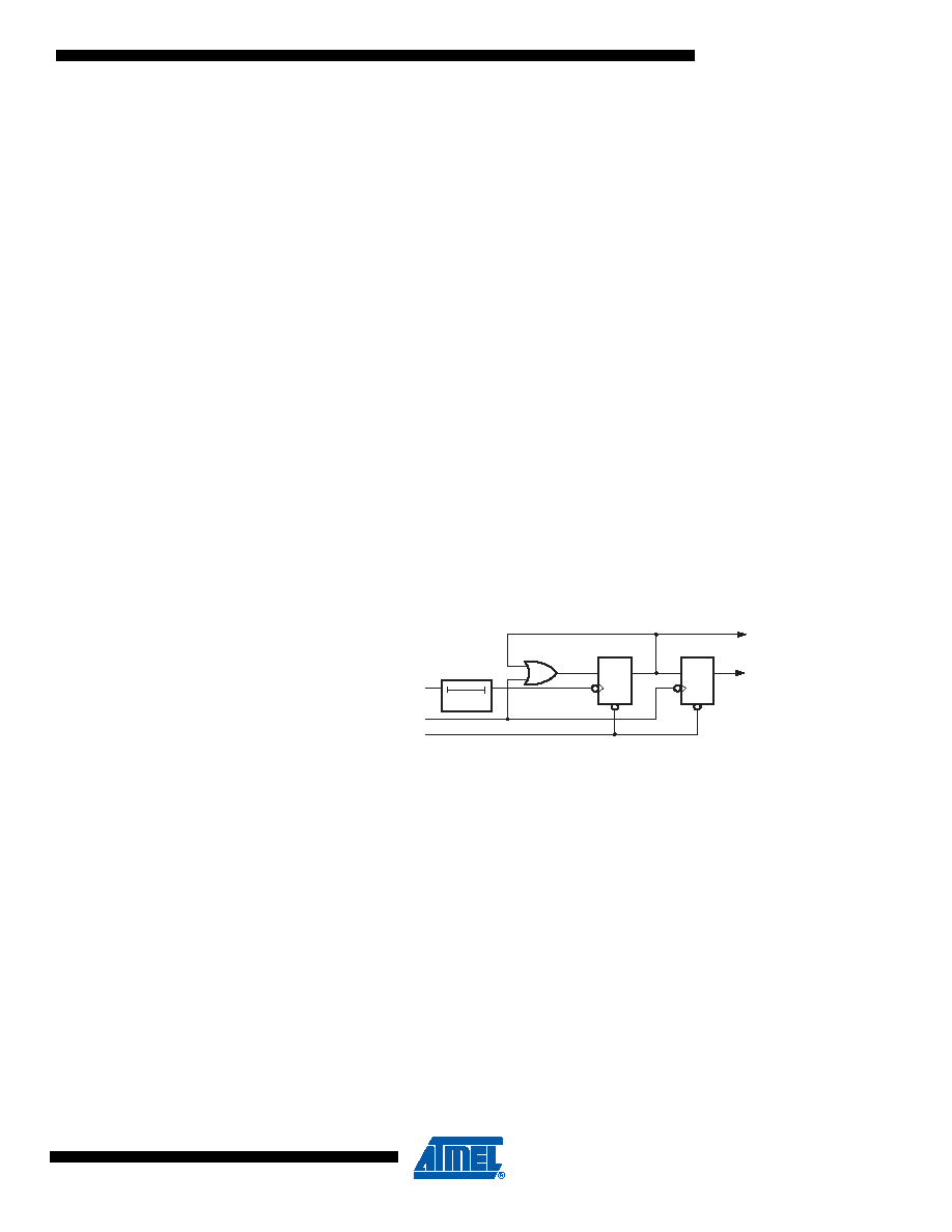
14.3.5
Start Condition Detector
The start condition detector is shown in Figure 14-6. The SDA line is delayed (in the range of 50
to 300 ns) to ensure valid sampling of the SCL line. The start condition detector is only enabled
in two-wire mode.
Figure 14-6. Start Condition Detector, Logic Diagram
The start condition detector works asynchronously and can therefore wake up the processor
from power-down sleep mode. However, the protocol used might have restrictions on the SCL
hold time. Therefore, when using this feature the oscillator start-up time (set by CKSEL fuses,
see “Clock Sources” on page 25) must also be taken into consideration. Refer to the description
of the USISIF bit on page 125 for further details.
14.3.6
Clock speed considerations
Maximum frequency for SCL and SCK is f
CK / 2. This is also the maximum data transmit and
receive rate in both two- and three-wire mode. In two-wire slave mode the Two-wire Clock Con-
trol Unit will hold the SCL low until the slave is ready to receive more data. This may reduce the
actual data rate in two-wire mode.
SDA
SCL
Write( USISIF)
CLOCK
HOLD
USISIF
DQ
CLR
DQ
CLR
相关PDF资料 |
PDF描述 |
|---|---|
| MAX4690EWE | IC SWITCH DUAL SPST 16SOIC |
| MAX4993ELB+T | IC SWITCH DPDT 10UDFN |
| MAX4992ELB+T | IC SWITCH DUAL SPDT 10UDFN |
| MAX4992EVB+ | IC SWITCH DUAL SPDT 10UTQFN |
| MAX4983EEVB+ | IC USB SWITCH DPDT 10UTQFN |
相关代理商/技术参数 |
参数描述 |
|---|---|
| DS72612RP100FPV | 功能描述:IC SUPERH MPU ROMLESS 176LQFP RoHS:是 类别:集成电路 (IC) >> 嵌入式 - 微控制器, 系列:SuperH® SH7200 标准包装:160 系列:S08 核心处理器:S08 芯体尺寸:8-位 速度:40MHz 连通性:I²C,LIN,SCI,SPI 外围设备:LCD,LVD,POR,PWM,WDT 输入/输出数:53 程序存储器容量:32KB(32K x 8) 程序存储器类型:闪存 EEPROM 大小:- RAM 容量:1.9K x 8 电压 - 电源 (Vcc/Vdd):2.7 V ~ 5.5 V 数据转换器:A/D 12x12b 振荡器型:内部 工作温度:-40°C ~ 105°C 封装/外壳:64-LQFP 包装:托盘 |
| DS72612RP80FPV | 功能描述:IC SUPERH MPU ROMLESS 176LQFP RoHS:是 类别:集成电路 (IC) >> 嵌入式 - 微控制器, 系列:SuperH® SH7200 标准包装:160 系列:S08 核心处理器:S08 芯体尺寸:8-位 速度:40MHz 连通性:I²C,LIN,SCI,SPI 外围设备:LCD,LVD,POR,PWM,WDT 输入/输出数:53 程序存储器容量:32KB(32K x 8) 程序存储器类型:闪存 EEPROM 大小:- RAM 容量:1.9K x 8 电压 - 电源 (Vcc/Vdd):2.7 V ~ 5.5 V 数据转换器:A/D 12x12b 振荡器型:内部 工作温度:-40°C ~ 105°C 封装/外壳:64-LQFP 包装:托盘 |
| DS72613RB120FPV | 功能描述:IC SUPERH MPU ROMLESS 176LQFP RoHS:是 类别:集成电路 (IC) >> 嵌入式 - 微控制器, 系列:SuperH® SH7200 标准包装:160 系列:S08 核心处理器:S08 芯体尺寸:8-位 速度:40MHz 连通性:I²C,LIN,SCI,SPI 外围设备:LCD,LVD,POR,PWM,WDT 输入/输出数:53 程序存储器容量:32KB(32K x 8) 程序存储器类型:闪存 EEPROM 大小:- RAM 容量:1.9K x 8 电压 - 电源 (Vcc/Vdd):2.7 V ~ 5.5 V 数据转换器:A/D 12x12b 振荡器型:内部 工作温度:-40°C ~ 105°C 封装/外壳:64-LQFP 包装:托盘 |
| DS72613RP80FPV | 功能描述:IC SUPERH MPU ROMLESS 176LQFP RoHS:是 类别:集成电路 (IC) >> 嵌入式 - 微控制器, 系列:SuperH® SH7200 标准包装:160 系列:S08 核心处理器:S08 芯体尺寸:8-位 速度:40MHz 连通性:I²C,LIN,SCI,SPI 外围设备:LCD,LVD,POR,PWM,WDT 输入/输出数:53 程序存储器容量:32KB(32K x 8) 程序存储器类型:闪存 EEPROM 大小:- RAM 容量:1.9K x 8 电压 - 电源 (Vcc/Vdd):2.7 V ~ 5.5 V 数据转换器:A/D 12x12b 振荡器型:内部 工作温度:-40°C ~ 105°C 封装/外壳:64-LQFP 包装:托盘 |
| DS7286-054NR1 WAF | 制造商:ON Semiconductor 功能描述: |
发布紧急采购,3分钟左右您将得到回复。