- 您现在的位置:买卖IC网 > PDF目录10917 > DS80C310-QNG+T&R (Maxim Integrated Products)IC MCU HI SPEED 25MHZ IND 44PLCC PDF资料下载
参数资料
| 型号: | DS80C310-QNG+T&R |
| 厂商: | Maxim Integrated Products |
| 文件页数: | 17/22页 |
| 文件大小: | 0K |
| 描述: | IC MCU HI SPEED 25MHZ IND 44PLCC |
| 标准包装: | 500 |
| 系列: | 80C |
| 核心处理器: | 8051 |
| 芯体尺寸: | 8-位 |
| 速度: | 25MHz |
| 连通性: | EBI/EMI,SIO,UART/USART |
| 外围设备: | 欠压检测/复位,POR |
| 输入/输出数: | 32 |
| 程序存储器类型: | ROMless |
| RAM 容量: | 256 x 8 |
| 电压 - 电源 (Vcc/Vdd): | 4.5 V ~ 5.5 V |
| 振荡器型: | 外部 |
| 工作温度: | -40°C ~ 85°C |
| 封装/外壳: | 44-LCC(J 形引线) |
| 包装: | 带卷 (TR) |
DS80C310
4 of 22
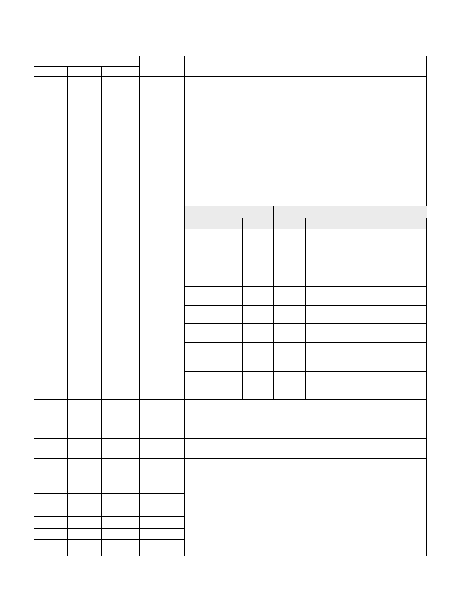
PIN
PDIP
PLCC
TQFP
NAME
FUNCTION
Port 3 (I/O). Port 3 functions as both an 8-bit bidirectional I/O port
and an alternate functional interface for external Interrupts, Serial
Port 0, Timer 0 and 1 Inputs,
RD and WR strobes. The reset
condition of Port 3 is with all bits at logic 1. In this state, a weak
pullup holds the port high. This condition also serves as an input
mode, since any external circuit that writes to the port will overcome
the weak pullup. When software writes a 0 to any port pin, the
DS80C310 will activate a strong pulldown that remains on until
either a 1 is written or a reset occurs. Writing a 1 after the port has
been at 0 will cause a strong transition driver to turn on, followed by
a weaker sustaining pullup. Once the momentary strong driver turns
off, the port once again becomes both the output high and input
state. The alternate modes of Port 3 are as follows:
PIN
PDIP
PLCC
TQFP
PORT
ALTERNATE
FUNCTION
10
11
5
P3.0
RXD0
Serial Port 0
Input
11
13
7
P3.1
TXD0
Serial Port 0
Output
12
14
8
P3.2
INT0
External Interrupt
0
13
15
9
P3.3
INT1
External Interrupt
1
14
16
10
P3.4
T0
Timer 0 External
Input
15
17
11
P3.5
T1
Timer 1 External
Input
16
18
12
P3.6
WR
External Data
Memory Write
Strobe
10–17
11,
13–19
5, 7–13
P3.0–P3.7
17
19
13
P3.7
RD
External Data
Memory Read
Strobe
18, 19
20, 21
14, 15
XTAL2,
XTAL1
Crystal Oscillator Pins. XTAL1 and XTAL2 provide support for
parallel resonant, AT-cut crystals. XTAL1 also acts as an input in
the event that an external clock source is used in place of a crystal.
XTAL2 serves as the output of the crystal amplifier.
20
1, 22,
23
16, 17,
39
GND
Digital Circuit Ground
21
24
18
A8(P2.0)
22
25
19
A9(P2.1)
23
26
20
A10(P2.2)
24
27
21
A11(P2.3)
25
28
22
A12(P2.4)
26
29
23
A13(P2.5)
27
30
24
A14(P2.6)
28
31
25
A15(P2.7)
Address Outputs (Port 2) (Output). Port 2 serves as the MSB for
external addressing. P2.7 is A15 and P2.0 is A8. The DS80C310
automatically places the MSB of an address on P2 for external ROM
and RAM access. Although Port 2 can be accessed like an ordinary
I/O port, the value stored on the Port 2 latch is never seen on the pins
(due to memory access). Therefore, writing to Port 2 in software is
only useful for the instructions MOVX A, @ Ri or MOVX @ Ri, A.
These instructions use the Port 2 internal latch to supply the external
address MSB; the Port 2 latch value is supplied as the address
information.
相关PDF资料 |
PDF描述 |
|---|---|
| VE-23M-IX-F4 | CONVERTER MOD DC/DC 10V 75W |
| VE-23M-IX-F3 | CONVERTER MOD DC/DC 10V 75W |
| VE-23M-IX-F2 | CONVERTER MOD DC/DC 10V 75W |
| VE-J3H-IY-B1 | CONVERTER MOD DC/DC 52V 50W |
| VE-J3F-IY-B1 | CONVERTER MOD DC/DC 72V 50W |
相关代理商/技术参数 |
参数描述 |
|---|---|
| DS80C320 | 制造商:MAXIM 制造商全称:Maxim Integrated Products 功能描述:High-Speed/Low-Power Microcontrollers |
| DS80C320_06 | 制造商:MAXIM 制造商全称:Maxim Integrated Products 功能描述:High-Speed/Low-Power Microcontrollers |
| DS80C320+ENL | 制造商:Maxim Integrated Products 功能描述:MCU 8BIT CISC ROMLESS 5V 44TQFP - Trays |
| DS80C320+FCG | 制造商:Maxim Integrated Products 功能描述:MICRO HI SPD 44PQFP 25MHZ PB-FREE - Trays |
| DS80C320+FNG | 制造商:Maxim Integrated Products 功能描述:MICRO HS 44MQFP 25MHZ IND PB-FREE - Trays |
发布紧急采购,3分钟左右您将得到回复。