- 您现在的位置:买卖IC网 > PDF目录1917 > DS90LV804TSQX/NOPB (National Semiconductor)IC BUFFER/REPEATR LVDS 4CH 32LLP PDF资料下载
参数资料
| 型号: | DS90LV804TSQX/NOPB |
| 厂商: | National Semiconductor |
| 文件页数: | 9/15页 |
| 文件大小: | 0K |
| 描述: | IC BUFFER/REPEATR LVDS 4CH 32LLP |
| 标准包装: | 4,500 |
| 类型: | 缓冲器 |
| Tx/Rx类型: | LVDS |
| 延迟时间: | 3.2ns |
| 电容 - 输入: | 3.5pF |
| 电源电压: | 3.15 V ~ 3.45 V |
| 电流 - 电源: | 140mA |
| 安装类型: | 表面贴装 |
| 封装/外壳: | 32-WFQFN 裸露焊盘 |
| 供应商设备封装: | 32-LLP-EP(5x5) |
| 包装: | 带卷 (TR) |
| 其它名称: | DS90LV804TSQX |
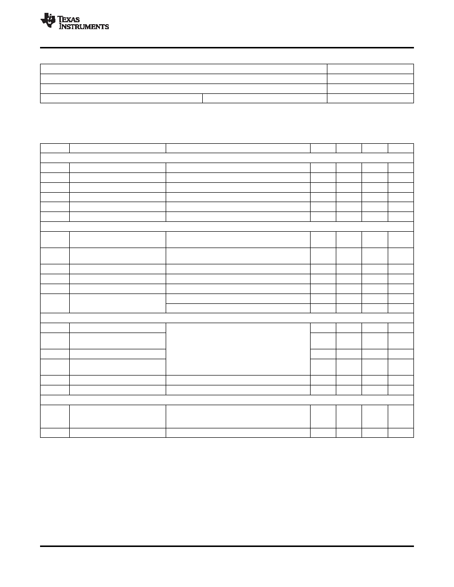
SNLS195L – SEPTEMBER 2005 – REVISED APRIL 2013
Recommended Operating Conditions
Supply Voltage (VCC)
3.15V to 3.45V
Input Voltage (VI)
(1)
0V to VDD
Output Voltage (VO)
0V to VDD
Operating Temperature (TA)
Industrial
40°C to +85°C
(1)
VID max < 2.4V
Electrical Characteristics
Over recommended operating supply and temperature ranges unless other specified.
Symbol
Parameter
Conditions
Min
Typ(1)
Max
Units
LVTTL DC SPECIFICATIONS (EN)
VIH
High Level Input Voltage
2.0
VDD
V
VIL
Low Level Input Voltage
GND
0.8
V
IIH
High Level Input Current
VIN = VDD = VDDMAX
10
+10
A
IIL
Low Level Input Current
VIN = VSS, VDD = VDDMAX
10
+10
A
CIN1
Input Capacitance
Any Digital Input Pin to VSS
3.5
pF
VCL
Input Clamp Voltage
ICL = 18 mA
1.5
0.8
V
LVDS INPUT DC SPECIFICATIONS (INn±)
VTH
VCM = 0.8V to 3.4V,
Differential Input High Threshold(2)
0
100
mV
VDD = 3.45V
VTL
VCM = 0.8V to 3.4V,
Differential Input Low Threshold(2)
100
0
mV
VDD = 3.45V
VID
Differential Input Voltage
VCM = 0.8V to 3.4V, VDD = 3.45V
100
2400
mV
VCMR
Common Mode Voltage Range
VID = 150 mV, VDD = 3.45V
0.05
3.40
V
CIN2
Input Capacitance
IN+ or IN
to VSS
3.5
pF
IIN
VIN = 3.45V, VDD = VDDMAX
10
+10
A
Input Current
VIN = 0V, VDD = VDDMAX
10
+10
A
LVDS OUTPUT DC SPECIFICATIONS (OUTn±)
VOD
Differential Output Voltage(2)
250
500
600
mV
ΔVOD
Change in VOD between
35
mV
Complementary States
RL = 100 external resistor between OUT+ and
OUT
VOS
Offset Voltage(3)
1.05
1.18
1.475
V
ΔVOS
Change in VOS between
35
mV
Complementary States
IOS
Output Short Circuit Current
OUT+ or OUT
Short to GND
60
90
mA
COUT2
Output Capacitance
OUT+ or OUT
to GND when TRI-STATE
5.5
pF
SUPPLY CURRENT (Static)
ICC
All inputs and outputs enabled and active,
Total Supply Current
terminated with external differential load of 100
117
140
mA
between OUT+ and OUT-.
ICCZ
TRI-STATE Supply Current
EN = 0V
2.7
6
mA
(1)
Typical parameters are measured at VDD = 3.3V, TA = 25°C. They are for reference purposes, and are not production-tested.
(2)
Differential output voltage VOD is defined as ABS(OUT+–OUT). Differential input voltage VID is defined as ABS(IN+–IN).
(3)
Output offset voltage VOS is defined as the average of the LVDS single-ended output voltages at logic high and logic low states.
Copyright 2005–2013, Texas Instruments Incorporated
3
Product Folder Links: DS90LV804
相关PDF资料 |
PDF描述 |
|---|---|
| DS9100-C+ | CONTACT TOUCH AND HOLD |
| DSP56301AG80B1 | IC DSP 24BIT 80MHZ GP 208-LQFP |
| DSP56301VF100 | IC DSP 24BIT FIXED-POINT 252-BGA |
| DSP56303VL100B1 | IC DSP 24BIT 100MHZ 196-BGA |
| DSP56311VF150B1 | IC DSP 24BIT 150MHZ 196-BGA |
相关代理商/技术参数 |
参数描述 |
|---|---|
| DS-90U | 制造商:Doublesight 功能描述:9" Smart USB LCD Monitor 制造商:DOUBLESIGHT 功能描述:9 USB LCD MONITOR USB 16:10 |
| DS90UA101-Q1 | 制造商:TI 制造商全称:Texas Instruments 功能描述:DS90UA101-Q1 Multi-Channel Digital Audio Link |
| DS90UA101-Q1EVM | 制造商:Texas Instruments 功能描述:DS90UA101-Q1EVM - Boxed Product (Development Kits) |
| DS90UA101TRTVJQ1 | 制造商:TI 制造商全称:Texas Instruments 功能描述:DS90UA101-Q1 Multi-Channel Digital Audio Link |
| DS90UA101TRTVRQ1 | 制造商:Texas Instruments 功能描述:IC SER/DESER 10-50MHZ 8B 32-WQFN |
发布紧急采购,3分钟左右您将得到回复。