- 您现在的位置:买卖IC网 > PDF目录1917 > DSP56321VF200R2 (Freescale Semiconductor)IC DSP 24BIT 200MHZ 196-BGA PDF资料下载
参数资料
| 型号: | DSP56321VF200R2 |
| 厂商: | Freescale Semiconductor |
| 文件页数: | 30/84页 |
| 文件大小: | 0K |
| 描述: | IC DSP 24BIT 200MHZ 196-BGA |
| 标准包装: | 750 |
| 系列: | DSP56K/Symphony |
| 类型: | 定点 |
| 接口: | 主机接口,SSI,SCI |
| 时钟速率: | 200MHz |
| 非易失内存: | ROM(576 B) |
| 芯片上RAM: | 576kB |
| 电压 - 输入/输出: | 3.30V |
| 电压 - 核心: | 1.60V |
| 工作温度: | -40°C ~ 100°C |
| 安装类型: | 表面贴装 |
| 封装/外壳: | 196-FBGA |
| 供应商设备封装: | 196-MAPBGA(15x15) |
| 包装: | 带卷 (TR) |
第1页第2页第3页第4页第5页第6页第7页第8页第9页第10页第11页第12页第13页第14页第15页第16页第17页第18页第19页第20页第21页第22页第23页第24页第25页第26页第27页第28页第29页当前第30页第31页第32页第33页第34页第35页第36页第37页第38页第39页第40页第41页第42页第43页第44页第45页第46页第47页第48页第49页第50页第51页第52页第53页第54页第55页第56页第57页第58页第59页第60页第61页第62页第63页第64页第65页第66页第67页第68页第69页第70页第71页第72页第73页第74页第75页第76页第77页第78页第79页第80页第81页第82页第83页第84页
DSP56321 Technical Data, Rev. 11
2-16
Freescale Semiconductor
Specifications
Notes:
1.
See the Programmer’s Model section in the chapter on the HI08 in the
DSP56321 Reference Manual.
2.
In the timing diagrams below, the controls pins are drawn as active low. The pin polarity is programmable.
3.
This timing is applicable only if two consecutive reads from one of these registers are executed.
4.
The data strobe is Host Read (HRD) or Host Write (HWR) in the Dual Data Strobe mode and Host Data Strobe (HDS) in the
Single Data Strobe mode.
5.
The read data strobe is HRD in the Dual Data Strobe mode and HDS in the Single Data Strobe mode.
6.
The write data strobe is HWR in the Dual Data Strobe mode and HDS in the Single Data Strobe mode.
7.
The host request is HREQ in the Single Host Request mode and HRRQ and HTRQ in the Double Host Request mode.
8.
The “Last Data Register” is the register at address $7, which is the last location to be read or written in data transfers. This is
RXL/TXL in the Big Endian mode (HLEND = 0; HLEND is the Interface Control Register bit 7—ICR[7]), or RXH/TXH in the
Little Endian mode (HLEND = 1).
9.
In this calculation, the host request signal is pulled up by a 4.7 k
resistor in the Open-drain mode.
10. VCCQH = 3.3 V ± 0.3 V, VCCQL = 1.6 V ± 0.1 V; TJ = –40°C to +100 °C, CL = 50 pF
11. This timing is applicable only if a read from the “Last Data Register” is followed by a read from the RXL, RXM, or RXH registers
without first polling RXDF or HREQ bits, or waiting for the assertion of the HREQ signal.
12. After the external host writes a new value to the ICR, the HI08 will be ready for operation after three DSP clock cycles (3
× Tc).
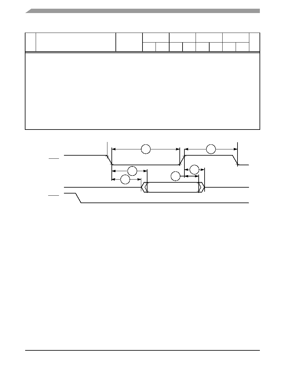
Figure 2-13.
Host Interrupt Vector Register (IVR) Read Timing Diagram
Table 2-10.
Host Interface Timings1,2,12 (Continued)
No.
Characteristic10
Expression
200 MHz
220 MHz
240 MHz
275 MHz
Uni
t
Min
Max
Min
Max
Min
Max
Min
Max
HACK
H[0–7]
HREQ
329
317
318
328
326
327
相关PDF资料 |
PDF描述 |
|---|---|
| DSP56852VFE | IC DSP 16BIT 120MHZ 81-MAPBGA |
| DSP56854FGE | IC DSP 16BIT 120MHZ 128-LQFP |
| DSP56855BUE | IC DSP 16BIT 120MHZ 100-LQFP |
| DSP56857BUE | IC DSP 16BIT 120MHZ 100-LQFP |
| DSP56858FVE | IC DSP 16BIT 120MHZ 144-LQFP |
相关代理商/技术参数 |
参数描述 |
|---|---|
| DSP56321VF220 | 功能描述:数字信号处理器和控制器 - DSP, DSC 220Mhz/440MMACS 220Mhz EFCOP RoHS:否 制造商:Microchip Technology 核心:dsPIC 数据总线宽度:16 bit 程序存储器大小:16 KB 数据 RAM 大小:2 KB 最大时钟频率:40 MHz 可编程输入/输出端数量:35 定时器数量:3 设备每秒兆指令数:50 MIPs 工作电源电压:3.3 V 最大工作温度:+ 85 C 封装 / 箱体:TQFP-44 安装风格:SMD/SMT |
| DSP56321VF240 | 功能描述:数字信号处理器和控制器 - DSP, DSC 240Mhz/480MMACS 240Mhz EFCOP RoHS:否 制造商:Microchip Technology 核心:dsPIC 数据总线宽度:16 bit 程序存储器大小:16 KB 数据 RAM 大小:2 KB 最大时钟频率:40 MHz 可编程输入/输出端数量:35 定时器数量:3 设备每秒兆指令数:50 MIPs 工作电源电压:3.3 V 最大工作温度:+ 85 C 封装 / 箱体:TQFP-44 安装风格:SMD/SMT |
| DSP56321VF275 | 功能描述:数字信号处理器和控制器 - DSP, DSC 275Mhz/550MMACS 275Mhz EFCOP RoHS:否 制造商:Microchip Technology 核心:dsPIC 数据总线宽度:16 bit 程序存储器大小:16 KB 数据 RAM 大小:2 KB 最大时钟频率:40 MHz 可编程输入/输出端数量:35 定时器数量:3 设备每秒兆指令数:50 MIPs 工作电源电压:3.3 V 最大工作温度:+ 85 C 封装 / 箱体:TQFP-44 安装风格:SMD/SMT |
| DSP56321VL200 | 功能描述:数字信号处理器和控制器 - DSP, DSC 24 BIT DSP PBFREE RoHS:否 制造商:Microchip Technology 核心:dsPIC 数据总线宽度:16 bit 程序存储器大小:16 KB 数据 RAM 大小:2 KB 最大时钟频率:40 MHz 可编程输入/输出端数量:35 定时器数量:3 设备每秒兆指令数:50 MIPs 工作电源电压:3.3 V 最大工作温度:+ 85 C 封装 / 箱体:TQFP-44 安装风格:SMD/SMT |
| DSP56321VL200R2 | 功能描述:数字信号处理器和控制器 - DSP, DSC 24 BIT DSP PBFREE RoHS:否 制造商:Microchip Technology 核心:dsPIC 数据总线宽度:16 bit 程序存储器大小:16 KB 数据 RAM 大小:2 KB 最大时钟频率:40 MHz 可编程输入/输出端数量:35 定时器数量:3 设备每秒兆指令数:50 MIPs 工作电源电压:3.3 V 最大工作温度:+ 85 C 封装 / 箱体:TQFP-44 安装风格:SMD/SMT |
发布紧急采购,3分钟左右您将得到回复。