- 您现在的位置:买卖IC网 > PDF目录1917 > DSP56854FGE (Freescale Semiconductor)IC DSP 16BIT 120MHZ 128-LQFP PDF资料下载
参数资料
| 型号: | DSP56854FGE |
| 厂商: | Freescale Semiconductor |
| 文件页数: | 26/60页 |
| 文件大小: | 0K |
| 描述: | IC DSP 16BIT 120MHZ 128-LQFP |
| 标准包装: | 72 |
| 系列: | 568xx |
| 核心处理器: | 56800E |
| 芯体尺寸: | 16-位 |
| 速度: | 120MHz |
| 连通性: | EBI/EMI,SCI,SPI,SSI |
| 外围设备: | DMA,POR,WDT |
| 输入/输出数: | 41 |
| 程序存储器容量: | 32KB(16K x 16) |
| 程序存储器类型: | SRAM |
| RAM 容量: | 16K x 16 |
| 电压 - 电源 (Vcc/Vdd): | 1.62 V ~ 1.98 V |
| 振荡器型: | 外部 |
| 工作温度: | -40°C ~ 85°C |
| 封装/外壳: | 128-LQFP |
| 包装: | 托盘 |
第1页第2页第3页第4页第5页第6页第7页第8页第9页第10页第11页第12页第13页第14页第15页第16页第17页第18页第19页第20页第21页第22页第23页第24页第25页当前第26页第27页第28页第29页第30页第31页第32页第33页第34页第35页第36页第37页第38页第39页第40页第41页第42页第43页第44页第45页第46页第47页第48页第49页第50页第51页第52页第53页第54页第55页第56页第57页第58页第59页第60页
56854 Technical Data, Rev. 6
32
Freescale Semiconductor
4.6 External Memory Interface Timing
The External Memory Interface is designed to access static memory and peripheral devices. Figure 4-10 shows
sample timing and parameters that are detailed in Table 4-11.
The timing of each parameter consists of both a fixed delay portion and a clock related portion; as well as user
controlled wait states. The equation:
t = D + P * (M + W)
should be used to determine the actual time of each parameter. The terms in the above equation are defined as:
t
parameter delay time
D fixed portion of the delay, due to on-chip path delays.
P the period of the system clock, which determines the execution rate of the part (i.e. when the device is
operating at 120 MHz, P = 8.33 ns).
M Fixed portion of a clock period inherent in the design. This number is adjusted to account for possible
clock duty cycle derating.
W the sum of the applicable wait state controls. See the “Wait State Controls” column of Table 4-11 for
the applicable controls for each parameter. See the EMI chapter of the 83x Peripheral Manual for
details of what each wait state field controls.
Some of the parameters contain two sets of numbers. These parameters have two different paths and clock edges
that must be considered. Check both sets of numbers and use the smaller result. The appropriate entry may change
if the operating frequency of the part changes.
The timing of write cycles is different when WWS = 0 than when WWS > 0. Therefore, some parameters contain
two sets of numbers to account for this difference. The “Wait States Configuration” column of Table 4-11 should
be used to make the appropriate selection.
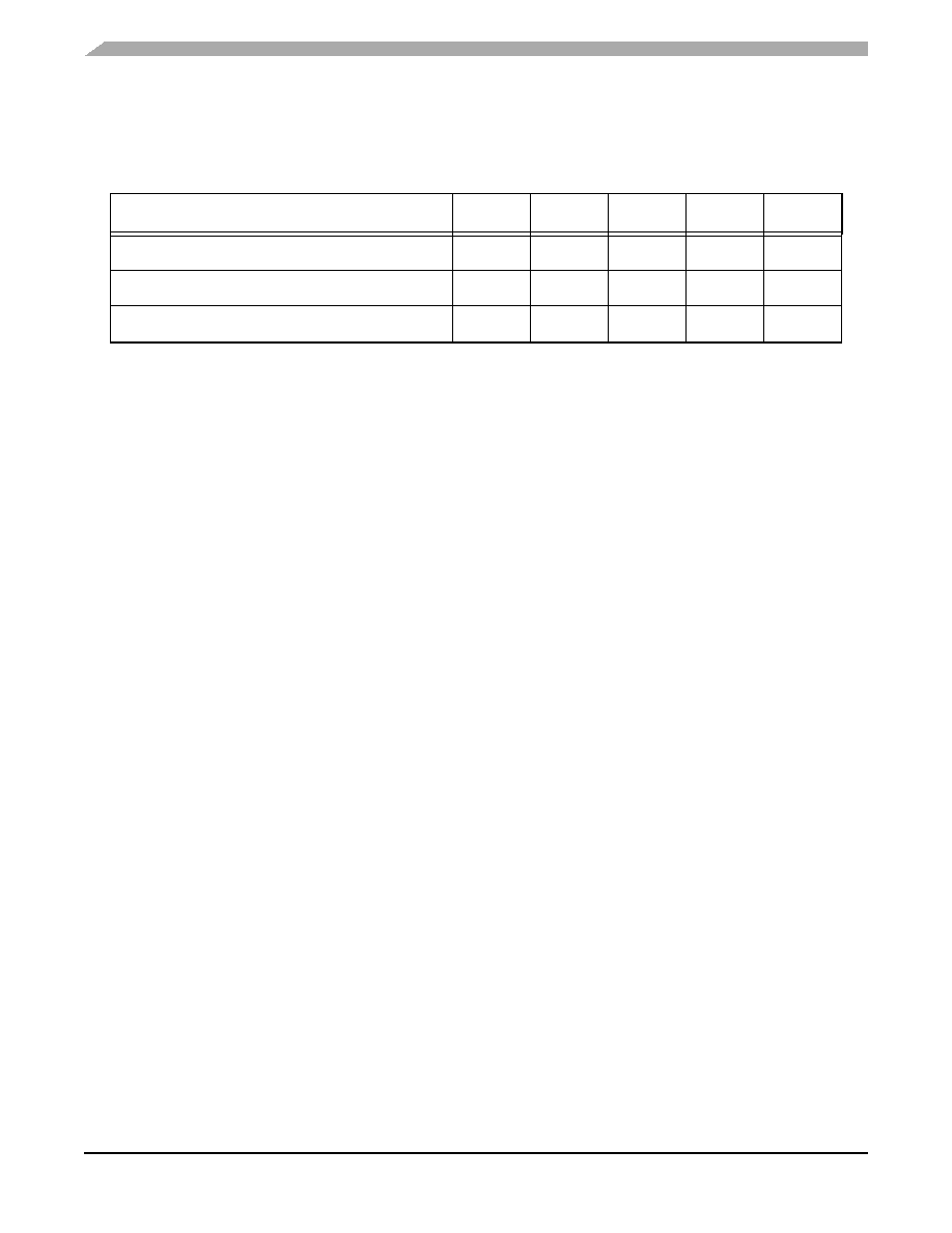
Table 4-6 PLL Timing
Operating Conditions: VSS = VSSIO = VSSA = 0 V, VDD = 1.62-1.98V, VDDIO = VDDA = 3.0–3.6V, TA = –40° to +120°C, CL ≤ 50pF, fop = 120MHz
Characteristic
Symbol
Min
Typ
Max
Unit
External reference crystal frequency for the PLL1
1.
An externally supplied reference clock should be as free as possible from any phase jitter for the PLL to work correctly.
The PLL is optimized for 4MHz input crystal.
fosc
2
4
MHz
PLL output frequency
fclk
40
—
240
MHz
PLL stabilization time 2
2.
This is the minimum time required after the PLL setup is changed to ensure reliable operation.
tplls
—
1
10
ms
相关PDF资料 |
PDF描述 |
|---|---|
| DSP56855BUE | IC DSP 16BIT 120MHZ 100-LQFP |
| DSP56857BUE | IC DSP 16BIT 120MHZ 100-LQFP |
| DSP56858FVE | IC DSP 16BIT 120MHZ 144-LQFP |
| DSP56F801FA80E | IC DSP 60MHZ 16KB FLASH 48-LQFP |
| DSP56F802TA80E | IC DSP 60MHZ 16KB FLASH 32-LQFP |
相关代理商/技术参数 |
参数描述 |
|---|---|
| DSP56854PB | 制造商:未知厂家 制造商全称:未知厂家 功能描述:56854 Digital Signal Processor Product Brief |
| DSP56855 | 制造商:FREESCALE 制造商全称:Freescale Semiconductor, Inc 功能描述:Digitial Signal Controller |
| DSP56855BU120 | 功能描述:数字信号处理器和控制器 - DSP, DSC 120Mhz/120MIPS RoHS:否 制造商:Microchip Technology 核心:dsPIC 数据总线宽度:16 bit 程序存储器大小:16 KB 数据 RAM 大小:2 KB 最大时钟频率:40 MHz 可编程输入/输出端数量:35 定时器数量:3 设备每秒兆指令数:50 MIPs 工作电源电压:3.3 V 最大工作温度:+ 85 C 封装 / 箱体:TQFP-44 安装风格:SMD/SMT |
| DSP56855BUE | 功能描述:数字信号处理器和控制器 - DSP, DSC 16 BIT HYBRID CONTROLLER RoHS:否 制造商:Microchip Technology 核心:dsPIC 数据总线宽度:16 bit 程序存储器大小:16 KB 数据 RAM 大小:2 KB 最大时钟频率:40 MHz 可编程输入/输出端数量:35 定时器数量:3 设备每秒兆指令数:50 MIPs 工作电源电压:3.3 V 最大工作温度:+ 85 C 封装 / 箱体:TQFP-44 安装风格:SMD/SMT |
| DSP56855E | 制造商:FREESCALE 制造商全称:Freescale Semiconductor, Inc 功能描述:16-bit Digital Signal Controllers |
发布紧急采购,3分钟左右您将得到回复。