- 您现在的位置:买卖IC网 > PDF目录1917 > DSPB56374AEC (Freescale Semiconductor)IC DSP 24BIT 150MHZ 52-LQFP PDF资料下载
参数资料
| 型号: | DSPB56374AEC |
| 厂商: | Freescale Semiconductor |
| 文件页数: | 62/64页 |
| 文件大小: | 0K |
| 描述: | IC DSP 24BIT 150MHZ 52-LQFP |
| 产品变化通告: | Product Discontinuation 24/Feb/2012 |
| 标准包装: | 160 |
| 系列: | DSP56K/Symphony |
| 类型: | 音频处理器 |
| 接口: | 主机接口,I²C,SAI,SPI |
| 时钟速率: | 150MHz |
| 非易失内存: | ROM(84 kB) |
| 芯片上RAM: | 54kB |
| 电压 - 输入/输出: | 3.30V |
| 电压 - 核心: | 1.25V |
| 工作温度: | -40°C ~ 110°C |
| 安装类型: | 表面贴装 |
| 封装/外壳: | 52-LQFP |
| 供应商设备封装: | 52-LQFP(10x10) |
| 包装: | 托盘 |
第1页第2页第3页第4页第5页第6页第7页第8页第9页第10页第11页第12页第13页第14页第15页第16页第17页第18页第19页第20页第21页第22页第23页第24页第25页第26页第27页第28页第29页第30页第31页第32页第33页第34页第35页第36页第37页第38页第39页第40页第41页第42页第43页第44页第45页第46页第47页第48页第49页第50页第51页第52页第53页第54页第55页第56页第57页第58页第59页第60页第61页当前第62页第63页第64页
Signal Groupings
DSP56374 Data Sheet, Rev. 4.2
Freescale Semiconductor
7
4.3
SCAN
4.4
Clock and PLL
PLLP_GND(1)
PLL Ground—The PLL ground should be provided with an extremely low-impedance path to
ground. This connection must be tied externally to all other chip ground connections. The user
must provide adequate external decoupling capacitors between PLLP_VDD and PLLP_GND.
PLLD_GND(1)
PLL Ground—The PLL ground should be provided with an extremely low-impedance path to
ground. This connection must be tied externally to all other chip ground connections. The user
must provide adequate external decoupling capacitors between PLLD_VDD and PLLD_GND.
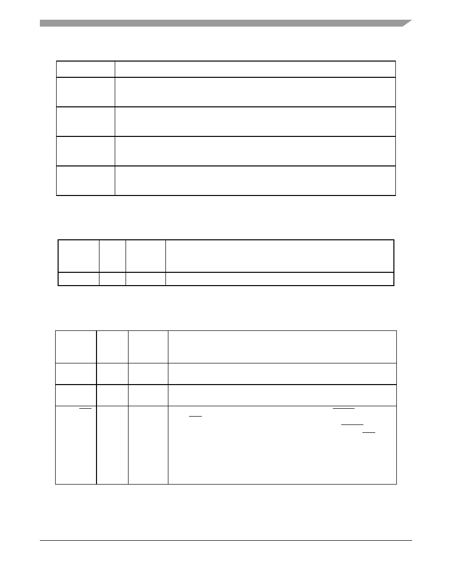
CORE_GND(4)
Core Ground—The Core ground should be provided with an extremely low-impedance path to
ground. This connection must be tied externally to all other chip ground connections. The user
must provide adequate external decoupling capacitors.
IO_GND(2)
SHI, ESAI, ESAI_1, WDT and Timer I/O Ground—IO_GND is the ground for the SHI, ESAI,
ESAI_1, WDT and Timer I/O. This connection must be tied externally to all other chip ground
connections. The user must provide adequate external decoupling capacitors.
Table 6. SCAN Signals
Signal
Name
Type
State
During
Reset
Signal Description
SCAN
Input
SCAN—Manufacturing test pin. This pin must be connected to ground.
Table 7. Clock and PLL Signals
Signal
Name
Type
State
during
Reset
Signal Description
EXTAL
Input
External Clock / Crystal Input—An external clock source must be connected
to EXTAL in order to supply the clock to the internal clock generator and PLL.
XTAL
Output
Chip Driven Crystal Output—Connects the internal Crystal Oscillator output to an external
crystal. If an external clock is used, leave XTAL unconnected.
PINIT/NMI
Input
PLL Initial/Nonmaskable Interrupt—During assertion of RESET, the value of
PINIT/NMI is written into the PLL Enable (PEN) bit of the PLL control register,
determining whether the PLL is enabled or disabled. After RESET
de-assertion and during normal instruction processing, the PINIT/NMI
Schmitt-trigger input is a negative-edge-triggered nonmaskable interrupt
(NMI) request internally synchronized to the internal system clock.
This pin has an internal pull up resistor.
This input is 5 V tolerant.
Table 5. Grounds (continued)
Ground Name
Description
相关PDF资料 |
PDF描述 |
|---|---|
| DSPB56720CAG | DSP 24BIT AUD 200MHZ 144-LQFP |
| DSPB56724AG | DSP 24BIT AUD 250MHZ 144-LQFP |
| DSPIC30F2010T-20E/MM | IC DSPIC MCU/DSP 12K 28QFN |
| DSPIC30F2020-30I/MMB32 | IC DSPIC MCU/DSP 12K 28QFN |
| DSPIC30F3011-20I/P | IC DSPIC MCU/DSP 24K 40DIP |
相关代理商/技术参数 |
参数描述 |
|---|---|
| DSPB56374AF | 功能描述:数字信号处理器和控制器 - DSP, DSC PB-FREE 80 LQFP 14X14MM RoHS:否 制造商:Microchip Technology 核心:dsPIC 数据总线宽度:16 bit 程序存储器大小:16 KB 数据 RAM 大小:2 KB 最大时钟频率:40 MHz 可编程输入/输出端数量:35 定时器数量:3 设备每秒兆指令数:50 MIPs 工作电源电压:3.3 V 最大工作温度:+ 85 C 封装 / 箱体:TQFP-44 安装风格:SMD/SMT |
| DSPB56374AF | 制造商:Freescale Semiconductor 功能描述:; Series:DSP56300; DSP Type:Static CMOS |
| DSPB56374AFC | 功能描述:数字信号处理器和控制器 - DSP, DSC 56374 80LQFP AUTOMOTIVE RoHS:否 制造商:Microchip Technology 核心:dsPIC 数据总线宽度:16 bit 程序存储器大小:16 KB 数据 RAM 大小:2 KB 最大时钟频率:40 MHz 可编程输入/输出端数量:35 定时器数量:3 设备每秒兆指令数:50 MIPs 工作电源电压:3.3 V 最大工作温度:+ 85 C 封装 / 箱体:TQFP-44 安装风格:SMD/SMT |
| DSPB56720AG | 功能描述:数字信号处理器和控制器 - DSP, DSC DSP56720 RoHS:否 制造商:Microchip Technology 核心:dsPIC 数据总线宽度:16 bit 程序存储器大小:16 KB 数据 RAM 大小:2 KB 最大时钟频率:40 MHz 可编程输入/输出端数量:35 定时器数量:3 设备每秒兆指令数:50 MIPs 工作电源电压:3.3 V 最大工作温度:+ 85 C 封装 / 箱体:TQFP-44 安装风格:SMD/SMT |
| DSPB56720CAG | 功能描述:数字信号处理器和控制器 - DSP, DSC 24-BIT 200MHz RoHS:否 制造商:Microchip Technology 核心:dsPIC 数据总线宽度:16 bit 程序存储器大小:16 KB 数据 RAM 大小:2 KB 最大时钟频率:40 MHz 可编程输入/输出端数量:35 定时器数量:3 设备每秒兆指令数:50 MIPs 工作电源电压:3.3 V 最大工作温度:+ 85 C 封装 / 箱体:TQFP-44 安装风格:SMD/SMT |
发布紧急采购,3分钟左右您将得到回复。