- 您现在的位置:买卖IC网 > PDF目录11291 > DSPIC30F2020-20E/SO (Microchip Technology)IC DSPIC MCU/DSP 12K 28SOIC PDF资料下载
参数资料
| 型号: | DSPIC30F2020-20E/SO |
| 厂商: | Microchip Technology |
| 文件页数: | 40/66页 |
| 文件大小: | 0K |
| 描述: | IC DSPIC MCU/DSP 12K 28SOIC |
| 产品培训模块: | Asynchronous Stimulus |
| 特色产品: | SMPS & Digital Power Conversion Solutions |
| 标准包装: | 27 |
| 系列: | dsPIC™ 30F |
| 核心处理器: | dsPIC |
| 芯体尺寸: | 16-位 |
| 速度: | 20 MIPS |
| 连通性: | I²C,IrDA,LIN,SPI,UART/USART |
| 外围设备: | 欠压检测/复位,POR,PWM,WDT |
| 输入/输出数: | 21 |
| 程序存储器容量: | 12KB(4K x 24) |
| 程序存储器类型: | 闪存 |
| RAM 容量: | 512 x 8 |
| 电压 - 电源 (Vcc/Vdd): | 3 V ~ 5.5 V |
| 数据转换器: | A/D 8x10b |
| 振荡器型: | 内部 |
| 工作温度: | -40°C ~ 125°C |
| 封装/外壳: | 28-SOIC(0.295",7.50mm 宽) |
| 包装: | 管件 |
| 产品目录页面: | 650 (CN2011-ZH PDF) |
| 配用: | DM300023-ND - KIT DEMO DSPICDEM SMPS BUCK DV164005-ND - KIT ICD2 SIMPLE SUIT W/USB CABLE |
第1页第2页第3页第4页第5页第6页第7页第8页第9页第10页第11页第12页第13页第14页第15页第16页第17页第18页第19页第20页第21页第22页第23页第24页第25页第26页第27页第28页第29页第30页第31页第32页第33页第34页第35页第36页第37页第38页第39页当前第40页第41页第42页第43页第44页第45页第46页第47页第48页第49页第50页第51页第52页第53页第54页第55页第56页第57页第58页第59页第60页第61页第62页第63页第64页第65页第66页
2010 Microchip Technology Inc.
DS70102K-page 45
dsPIC30F Flash Programming Specification
11.8
Writing Code Memory
The procedure for writing code memory is similar to the
procedure for clearing the Configuration registers,
except that 32 instruction words are programmed at a
time. To facilitate this operation, working registers
W0:W5 are used as temporary holding registers for the
data to be programmed.
Table 11-8 shows the ICSP programming details,
including the serial pattern with the ICSP command
code, which must be transmitted Least Significant bit
first using the PGC and PGD pins (see Figure 11-2). In
Step 1, the Reset vector is exited. In Step 2, the
NVMCON register is initialized for single-panel
programming of code memory. In Step 3, the 24-bit
starting destination address for programming is loaded
into the TBLPAG register and W7 register. The upper
byte of the starting destination address is stored to
TBLPAG, while the lower 16 bits of the destination
address are stored to W7.
To minimize the programming time, the same packed
instruction format that the programming executive uses
is utilized (Figure 8-2). In Step 4, four packed
instruction words are stored to working registers
W0:W5 using the MOV instruction and the read pointer
W6 is initialized. The contents of W0:W5 holding the
packed instruction word data is shown in Figure 11-4.
In Step 5, eight TBLWT instructions are used to copy the
data from W0:W5 to the write latches of code memory.
Since code memory is programmed 32 instruction
words at a time, Steps 4 and 5 are repeated eight times
to load all the write latches (Step 6).
After the write latches are loaded, programming is
initiated by writing to the NVMKEY and NVMCON
registers in Steps 7 and 8. In Step 9, the internal PC is
reset to 0x100. This is a precautionary measure to
prevent the PC from incrementing into unimplemented
memory when large devices are being programmed.
Lastly, in Step 10, Steps 2-9 are repeated until all of
code memory is programmed.
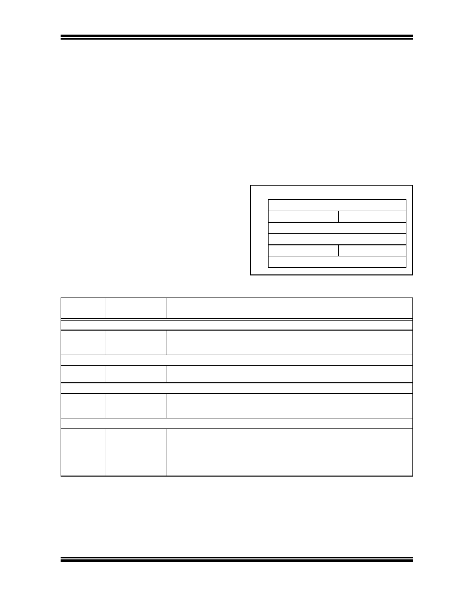
FIGURE 11-5:
PACKED INSTRUCTION
WORDS IN W0:W5
15
8
7
0
W0
lsw0
W1
MSB1
MSB0
W2
lsw1
W3
lsw2
W4
MSB3
MSB2
W5
lsw3
TABLE 11-8:
SERIAL INSTRUCTION EXECUTION FOR WRITING CODE MEMORY
Command
(Binary)
Data
(Hexadecimal)
Description
Step 1: Exit the Reset vector.
0000
040100
000000
GOTO 0x100
NOP
Step 2: Set the NVMCON to program 32 instruction words.
0000
24001A
883B0A
MOV
#0x4001, W10
MOV
W10, NVMCON
Step 3: Initialize the write pointer (W7) for TBLWT instruction.
0000
200xx0
880190
2xxxx7
MOV
#<DestinationAddress23:16>, W0
MOV
W0, TBLPAG
MOV
#<DestinationAddress15:0>, W7
Step 4: Initialize the read pointer (W6) and load W0:W5 with the next 4 instruction words to program.
0000
2xxxx0
2xxxx1
2xxxx2
2xxxx3
2xxxx4
2xxxx5
MOV
#<LSW0>, W0
MOV
#<MSB1:MSB0>, W1
MOV
#<LSW1>, W2
MOV
#<LSW2>, W3
MOV
#<MSB3:MSB2>, W4
MOV
#<LSW3>, W5
相关PDF资料 |
PDF描述 |
|---|---|
| PIC24HJ128GP502-E/SO | IC PIC MCU FLASH 128K 28-SOIC |
| PIC18F8520T-I/PT | IC PIC MCU FLASH 16KX16 80-TQFP |
| PIC18F4220-E/ML | IC MCU FLASH 2KX16 EEPROM 44QFN |
| DG2038DS-T1-E3 | IC SWITCH DUAL SPDT SOT23-8 |
| PIC18LF6520T-I/PT | IC MCU FLASH 16KX16 EEPROM64TQFP |
相关代理商/技术参数 |
参数描述 |
|---|---|
| dsPIC30F2020-30I/MM | 功能描述:数字信号处理器和控制器 - DSP, DSC 12KB 512bytes-RAM 30MIPS 21I/O RoHS:否 制造商:Microchip Technology 核心:dsPIC 数据总线宽度:16 bit 程序存储器大小:16 KB 数据 RAM 大小:2 KB 最大时钟频率:40 MHz 可编程输入/输出端数量:35 定时器数量:3 设备每秒兆指令数:50 MIPs 工作电源电压:3.3 V 最大工作温度:+ 85 C 封装 / 箱体:TQFP-44 安装风格:SMD/SMT |
| DSPIC30F2020-30I/MMB32 | 功能描述:IC DSPIC MCU/DSP 12K 28QFN RoHS:是 类别:集成电路 (IC) >> 嵌入式 - 微控制器, 系列:dsPIC™ 30F 产品培训模块:The Ultra-Low Power MSP430 MSP430 Overview MSP430 Design Tools MSP430 Peripherals MSP430 for Utility Metering Solutions MSP430: How to JTAG MSP430, How To Use the Clock System Grace Software Graphical User Interface MCU Overview Driver Library MSP430Ware Overview 标准包装:60 系列:MSP430F2xx 核心处理器:RISC 芯体尺寸:16-位 速度:12MHz 连通性:SPI,UART/USART 外围设备:欠压检测/复位,PWM,WDT 输入/输出数:11 程序存储器容量:4KB(4K x 8) 程序存储器类型:闪存 EEPROM 大小:- RAM 容量:256 x 8 电压 - 电源 (Vcc/Vdd):1.8 V ~ 3.6 V 数据转换器:A/D 3x24b 振荡器型:内部 工作温度:-40°C ~ 85°C 封装/外壳:24-TSSOP(0.173",4.40mm 宽) 包装:管件 |
| dsPIC30F2020-30I/SO | 功能描述:数字信号处理器和控制器 - DSP, DSC 12KB 512bytes-RAM 30MIPS 21I/O RoHS:否 制造商:Microchip Technology 核心:dsPIC 数据总线宽度:16 bit 程序存储器大小:16 KB 数据 RAM 大小:2 KB 最大时钟频率:40 MHz 可编程输入/输出端数量:35 定时器数量:3 设备每秒兆指令数:50 MIPs 工作电源电压:3.3 V 最大工作温度:+ 85 C 封装 / 箱体:TQFP-44 安装风格:SMD/SMT |
| dsPIC30F2020-30I/SP | 功能描述:数字信号处理器和控制器 - DSP, DSC 12KB 512bytes-RAM 30MIPS 21I/O RoHS:否 制造商:Microchip Technology 核心:dsPIC 数据总线宽度:16 bit 程序存储器大小:16 KB 数据 RAM 大小:2 KB 最大时钟频率:40 MHz 可编程输入/输出端数量:35 定时器数量:3 设备每秒兆指令数:50 MIPs 工作电源电压:3.3 V 最大工作温度:+ 85 C 封装 / 箱体:TQFP-44 安装风格:SMD/SMT |
| DSPIC30F2020AT-20E | 制造商:MICROCHIP 制造商全称:Microchip Technology 功能描述:28/44-Pin High-Performance Switch Mode Power Supply Digital Signal Controllers |
发布紧急采购,3分钟左右您将得到回复。