- 您现在的位置:买卖IC网 > PDF目录11291 > DSPIC30F2020-20E/SO (Microchip Technology)IC DSPIC MCU/DSP 12K 28SOIC PDF资料下载
参数资料
| 型号: | DSPIC30F2020-20E/SO |
| 厂商: | Microchip Technology |
| 文件页数: | 56/66页 |
| 文件大小: | 0K |
| 描述: | IC DSPIC MCU/DSP 12K 28SOIC |
| 产品培训模块: | Asynchronous Stimulus |
| 特色产品: | SMPS & Digital Power Conversion Solutions |
| 标准包装: | 27 |
| 系列: | dsPIC™ 30F |
| 核心处理器: | dsPIC |
| 芯体尺寸: | 16-位 |
| 速度: | 20 MIPS |
| 连通性: | I²C,IrDA,LIN,SPI,UART/USART |
| 外围设备: | 欠压检测/复位,POR,PWM,WDT |
| 输入/输出数: | 21 |
| 程序存储器容量: | 12KB(4K x 24) |
| 程序存储器类型: | 闪存 |
| RAM 容量: | 512 x 8 |
| 电压 - 电源 (Vcc/Vdd): | 3 V ~ 5.5 V |
| 数据转换器: | A/D 8x10b |
| 振荡器型: | 内部 |
| 工作温度: | -40°C ~ 125°C |
| 封装/外壳: | 28-SOIC(0.295",7.50mm 宽) |
| 包装: | 管件 |
| 产品目录页面: | 650 (CN2011-ZH PDF) |
| 配用: | DM300023-ND - KIT DEMO DSPICDEM SMPS BUCK DV164005-ND - KIT ICD2 SIMPLE SUIT W/USB CABLE |
第1页第2页第3页第4页第5页第6页第7页第8页第9页第10页第11页第12页第13页第14页第15页第16页第17页第18页第19页第20页第21页第22页第23页第24页第25页第26页第27页第28页第29页第30页第31页第32页第33页第34页第35页第36页第37页第38页第39页第40页第41页第42页第43页第44页第45页第46页第47页第48页第49页第50页第51页第52页第53页第54页第55页当前第56页第57页第58页第59页第60页第61页第62页第63页第64页第65页第66页
dsPIC30F Flash Programming Specification
DS70102K-page 6
2010 Microchip Technology Inc.
5.2
Entering Enhanced ICSP Mode
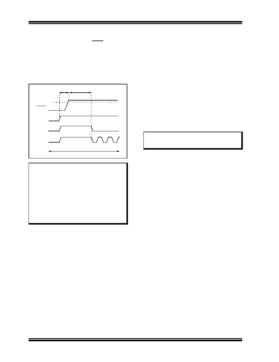
The Enhanced ICSP mode is entered by holding PGC
and PGD high, and then raising MCLR/VPP to VIHH
(high voltage), as illustrated in Figure 5-2. In this mode,
the code memory, data EEPROM and Configuration
bits can be efficiently programmed using the program-
ming executive commands that are serially transferred
using PGC and PGD.
FIGURE 5-2:
ENTERING ENHANCED
ICSP MODE
5.3
Chip Erase
Before a chip can be programmed, it must be erased.
The Bulk Erase command (ERASEB) is used to perform
this task. Executing this command with the MS
command field set to 0x3 erases all code memory, data
EEPROM and code-protect Configuration bits. The
Chip Erase process sets all bits in these three memory
regions to ‘1’.
Since non-code-protect Configuration bits cannot be
erased, they must be manually set to ‘1’ using multiple
PROGC commands. One PROGC command must be
sent for each Configuration register (see Section 5.7
If Advanced Security features are enabled, then indi-
vidual Segment Erase operations would need to be
performed, depending on which segment needs to be
programmed at a given stage of system programming.
The user should have the flexibility to select specific
segments for programming.
Note:
The Device ID registers cannot be erased.
These registers remain intact after a Chip
Erase is performed.
5.4
Blank Check
The term “Blank Check” means to verify that the device
has been successfully erased and has no programmed
memory cells. A blank or erased memory cell reads as
‘1’. The following memories must be blank checked:
All implemented code memory
All implemented data EEPROM
All Configuration bits (for their default value)
The Device ID registers (0xFF0000:0xFF0002) can be
ignored by the Blank Check since this region stores
device information that cannot be erased. Additionally,
all unimplemented memory space should be ignored
from the Blank Check.
The QBLANK command is used for the Blank Check. It
determines if the code memory and data EEPROM are
erased by testing these memory regions. A ‘BLANK’ or
‘NOT BLANK’ response is returned. The READD
command is used to read the Configuration registers. If
it is determined that the device is not blank, it must be
erased (see Section 5.3 “Chip Erase”) before
attempting to program the chip.
Note 1: The sequence that places the device into
Enhanced ICSP mode places all unused
I/Os in the high-impedance state.
2: Before entering Enhanced ICSP mode,
clock switching must be disabled using
ICSP, by programming the FCKSM<1:0>
bits in the FOSC Configuration register to
‘11’ or ‘10’.
3: When in Enhanced ICSP mode, the SPI
output pin (SDO1) will toggle while the
device is being programmed.
MCLR/VPP
P7
PGD
PGD = Input
PGC
VDD
VIHH
P6
相关PDF资料 |
PDF描述 |
|---|---|
| PIC24HJ128GP502-E/SO | IC PIC MCU FLASH 128K 28-SOIC |
| PIC18F8520T-I/PT | IC PIC MCU FLASH 16KX16 80-TQFP |
| PIC18F4220-E/ML | IC MCU FLASH 2KX16 EEPROM 44QFN |
| DG2038DS-T1-E3 | IC SWITCH DUAL SPDT SOT23-8 |
| PIC18LF6520T-I/PT | IC MCU FLASH 16KX16 EEPROM64TQFP |
相关代理商/技术参数 |
参数描述 |
|---|---|
| dsPIC30F2020-30I/MM | 功能描述:数字信号处理器和控制器 - DSP, DSC 12KB 512bytes-RAM 30MIPS 21I/O RoHS:否 制造商:Microchip Technology 核心:dsPIC 数据总线宽度:16 bit 程序存储器大小:16 KB 数据 RAM 大小:2 KB 最大时钟频率:40 MHz 可编程输入/输出端数量:35 定时器数量:3 设备每秒兆指令数:50 MIPs 工作电源电压:3.3 V 最大工作温度:+ 85 C 封装 / 箱体:TQFP-44 安装风格:SMD/SMT |
| DSPIC30F2020-30I/MMB32 | 功能描述:IC DSPIC MCU/DSP 12K 28QFN RoHS:是 类别:集成电路 (IC) >> 嵌入式 - 微控制器, 系列:dsPIC™ 30F 产品培训模块:The Ultra-Low Power MSP430 MSP430 Overview MSP430 Design Tools MSP430 Peripherals MSP430 for Utility Metering Solutions MSP430: How to JTAG MSP430, How To Use the Clock System Grace Software Graphical User Interface MCU Overview Driver Library MSP430Ware Overview 标准包装:60 系列:MSP430F2xx 核心处理器:RISC 芯体尺寸:16-位 速度:12MHz 连通性:SPI,UART/USART 外围设备:欠压检测/复位,PWM,WDT 输入/输出数:11 程序存储器容量:4KB(4K x 8) 程序存储器类型:闪存 EEPROM 大小:- RAM 容量:256 x 8 电压 - 电源 (Vcc/Vdd):1.8 V ~ 3.6 V 数据转换器:A/D 3x24b 振荡器型:内部 工作温度:-40°C ~ 85°C 封装/外壳:24-TSSOP(0.173",4.40mm 宽) 包装:管件 |
| dsPIC30F2020-30I/SO | 功能描述:数字信号处理器和控制器 - DSP, DSC 12KB 512bytes-RAM 30MIPS 21I/O RoHS:否 制造商:Microchip Technology 核心:dsPIC 数据总线宽度:16 bit 程序存储器大小:16 KB 数据 RAM 大小:2 KB 最大时钟频率:40 MHz 可编程输入/输出端数量:35 定时器数量:3 设备每秒兆指令数:50 MIPs 工作电源电压:3.3 V 最大工作温度:+ 85 C 封装 / 箱体:TQFP-44 安装风格:SMD/SMT |
| dsPIC30F2020-30I/SP | 功能描述:数字信号处理器和控制器 - DSP, DSC 12KB 512bytes-RAM 30MIPS 21I/O RoHS:否 制造商:Microchip Technology 核心:dsPIC 数据总线宽度:16 bit 程序存储器大小:16 KB 数据 RAM 大小:2 KB 最大时钟频率:40 MHz 可编程输入/输出端数量:35 定时器数量:3 设备每秒兆指令数:50 MIPs 工作电源电压:3.3 V 最大工作温度:+ 85 C 封装 / 箱体:TQFP-44 安装风格:SMD/SMT |
| DSPIC30F2020AT-20E | 制造商:MICROCHIP 制造商全称:Microchip Technology 功能描述:28/44-Pin High-Performance Switch Mode Power Supply Digital Signal Controllers |
发布紧急采购,3分钟左右您将得到回复。