- 您现在的位置:买卖IC网 > PDF目录3827 > DSPIC33FJ128GP306-I/PT (Microchip Technology)IC DSPIC MCU/DSP 128K 64TQFP PDF资料下载
参数资料
| 型号: | DSPIC33FJ128GP306-I/PT |
| 厂商: | Microchip Technology |
| 文件页数: | 89/90页 |
| 文件大小: | 0K |
| 描述: | IC DSPIC MCU/DSP 128K 64TQFP |
| 产品培训模块: | dsPIC33F DMAC Introduction to dsPIC33F Architecture Part 1 Asynchronous Stimulus Introduction to dsPIC33F Architecture Part 2 |
| 特色产品: | PIC24FJ/33FJ MCUs & dsPIC? DSCs |
| 标准包装: | 160 |
| 系列: | dsPIC™ 33F |
| 核心处理器: | dsPIC |
| 芯体尺寸: | 16-位 |
| 速度: | 40 MIP |
| 连通性: | I²C,IrDA,LIN,SPI,UART/USART |
| 外围设备: | AC'97,欠压检测/复位,DMA,I²S,POR,PWM,WDT |
| 输入/输出数: | 53 |
| 程序存储器容量: | 128KB(128K x 8) |
| 程序存储器类型: | 闪存 |
| RAM 容量: | 16K x 8 |
| 电压 - 电源 (Vcc/Vdd): | 3 V ~ 3.6 V |
| 数据转换器: | A/D 18x10b/12b |
| 振荡器型: | 内部 |
| 工作温度: | -40°C ~ 85°C |
| 封装/外壳: | 64-TQFP |
| 包装: | 托盘 |
| 产品目录页面: | 654 (CN2011-ZH PDF) |
| 配用: | 876-1001-ND - DSPIC33 BREAKOUT BOARD DM300024-ND - KIT DEMO DSPICDEM 1.1 DV164033-ND - KIT START EXPLORER 16 MPLAB ICD2 MA330012-ND - MODULE DSPIC33 100P TO 84QFP MA330011-ND - MODULE DSPIC33 100P TO 100QFP DM300019-ND - BOARD DEMO DSPICDEM 80L STARTER DM240001-ND - BOARD DEMO PIC24/DSPIC33/PIC32 AC164327-ND - MODULE SKT FOR 64TQFP DV164005-ND - KIT ICD2 SIMPLE SUIT W/USB CABLE |
第1页第2页第3页第4页第5页第6页第7页第8页第9页第10页第11页第12页第13页第14页第15页第16页第17页第18页第19页第20页第21页第22页第23页第24页第25页第26页第27页第28页第29页第30页第31页第32页第33页第34页第35页第36页第37页第38页第39页第40页第41页第42页第43页第44页第45页第46页第47页第48页第49页第50页第51页第52页第53页第54页第55页第56页第57页第58页第59页第60页第61页第62页第63页第64页第65页第66页第67页第68页第69页第70页第71页第72页第73页第74页第75页第76页第77页第78页第79页第80页第81页第82页第83页第84页第85页第86页第87页第88页当前第89页第90页
2005 Microchip Technology Inc.
Preliminary
DS70155C-page 7
dsPIC33F
3.0
CPU ARCHITECTURE
3.1
Overview
The dsPIC33F CPU module has a 16-bit (data)
modified Harvard architecture with an enhanced
instruction set, including significant support for DSP.
The CPU has a 24-bit instruction word with a variable
length opcode field. The Program Counter (PC) is
23 bits wide and addresses up to 4M x 24 bits of user
program memory space. The actual amount of program
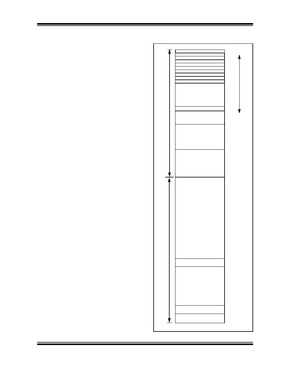
memory implemented, as illustrated in Figure 3-1,
varies from one device to another. A single-cycle
instruction prefetch mechanism is used to help
maintain
throughput
and
provides
predictable
execution. All instructions execute in a single cycle,
with the exception of instructions that change the
program
flow,
the
double
word
move
(MOV.D)
instruction and the table instructions. Overhead-free
program loop constructs are supported using the DO
and
REPEAT
instructions,
both
of
which
are
interruptible at any point.
The dsPIC33F devices have sixteen 16-bit working
registers in the programmer’s model. Each of the
working registers can serve as a data, address or
address offset register. The 16th working register
(W15) operates as a software Stack Pointer (SP) for
interrupts and calls.
The dsPIC33F instruction set has two classes of
instructions: the MCU class of instructions and the DSP
class of instructions. These two instruction classes are
seamlessly
integrated
into
a
single
CPU.
The
instruction set includes many addressing modes and is
designed for optimum C compiler efficiency.
3.1.1
DATA MEMORY OVERVIEW
The data space can be addressed as 32K words or
64 Kbytes and is split into two blocks, referred to as X
and Y data memory. Each memory block has its own
independent Address Generation Unit (AGU). The
MCU class of instructions operates solely through the
X memory AGU, which accesses the entire memory
map as one linear data space. Certain DSP instructions
operate through the X and Y AGUs to support dual
operand reads, which splits the data address space
into two parts. The X and Y data space boundary is
device specific.
The upper 32 Kbytes of the data space memory map
can optionally be mapped into program space at any
16K program word boundary defined by the 8-bit
Program Space Visibility Page (PSVPAG) register. The
program-to-data space mapping feature lets any
instruction access program space as if it were data
space.
The data space includes 2 Kbytes of DMA RAM, which
is primarily used for DMA data transfers, but may be
used as general purpose RAM.
FIGURE 3-1:
PROGRAM SPACE
MEMORY MAP
Reset – Target Address
U
s
er
Me
mo
ry
Sp
a
c
e
000000
0000FE
Reserved
000002
000100
Device Configuration
User Flash
Program Memory
02AC00
02ABFE
C
o
nf
ig
ur
a
ti
o
n
Me
mo
ry
S
pace
Osc. Fail Trap Vector
Address Error Trap Vector
Stack Error Trap Vector
Math Error Trap Vector
DMA Error Vector
Reserved Vector
Interrupt Vector Table
(87296 x 24-bit)
800000
F80000
Registers (12 x 8-bit)
F80016
F80018
FFFFFE
F7FFFE
Reserved
000014
Ve
c
to
r
Reset – GOTO Instruction
000004
Reserved
7FFFFE
Reserved
000200
0001FE
000104
Alternate Vector Table
Reserved
Ta
b
le
s
Reserved Vector
Device ID (2 x 16-bit)
Reserved
FEFFFE
FF0000
FF0002
FF0004
相关PDF资料 |
PDF描述 |
|---|---|
| PIC24HJ128GP306-I/PT | IC PIC MCU FLASH 128KB 64TQFP |
| PIC16F873-20/SO | IC MCU FLASH 4KX14 EE 28SOIC |
| PIC18F4431-I/P | IC PIC MCU FLASH 8KX16 40DIP |
| PIC16F777-I/P | IC PIC MCU FLASH 8KX14 40DIP |
| PIC16F873-20/SP | IC MCU FLASH 4KX14 EE 28DIP |
相关代理商/技术参数 |
参数描述 |
|---|---|
| dsPIC33FJ128GP306T-I/PT | 功能描述:数字信号处理器和控制器 - DSP, DSC 40MIPS 128KB RoHS:否 制造商:Microchip Technology 核心:dsPIC 数据总线宽度:16 bit 程序存储器大小:16 KB 数据 RAM 大小:2 KB 最大时钟频率:40 MHz 可编程输入/输出端数量:35 定时器数量:3 设备每秒兆指令数:50 MIPs 工作电源电压:3.3 V 最大工作温度:+ 85 C 封装 / 箱体:TQFP-44 安装风格:SMD/SMT |
| dsPIC33FJ128GP310A-E/PF | 功能描述:数字信号处理器和控制器 - DSP, DSC 16Bit 40MIPS 128KB Flash RoHS:否 制造商:Microchip Technology 核心:dsPIC 数据总线宽度:16 bit 程序存储器大小:16 KB 数据 RAM 大小:2 KB 最大时钟频率:40 MHz 可编程输入/输出端数量:35 定时器数量:3 设备每秒兆指令数:50 MIPs 工作电源电压:3.3 V 最大工作温度:+ 85 C 封装 / 箱体:TQFP-44 安装风格:SMD/SMT |
| dsPIC33FJ128GP310A-E/PT | 功能描述:数字信号处理器和控制器 - DSP, DSC 16Bit MCU/DSP 40MIPS 128KB FLASH RoHS:否 制造商:Microchip Technology 核心:dsPIC 数据总线宽度:16 bit 程序存储器大小:16 KB 数据 RAM 大小:2 KB 最大时钟频率:40 MHz 可编程输入/输出端数量:35 定时器数量:3 设备每秒兆指令数:50 MIPs 工作电源电压:3.3 V 最大工作温度:+ 85 C 封装 / 箱体:TQFP-44 安装风格:SMD/SMT |
| dsPIC33FJ128GP310A-I/PF | 功能描述:数字信号处理器和控制器 - DSP, DSC 16Bit 40MIPS 128KB Flash RoHS:否 制造商:Microchip Technology 核心:dsPIC 数据总线宽度:16 bit 程序存储器大小:16 KB 数据 RAM 大小:2 KB 最大时钟频率:40 MHz 可编程输入/输出端数量:35 定时器数量:3 设备每秒兆指令数:50 MIPs 工作电源电压:3.3 V 最大工作温度:+ 85 C 封装 / 箱体:TQFP-44 安装风格:SMD/SMT |
| dsPIC33FJ128GP310A-I/PT | 功能描述:数字信号处理器和控制器 - DSP, DSC 16Bit 40MIPS 128KB Flash RoHS:否 制造商:Microchip Technology 核心:dsPIC 数据总线宽度:16 bit 程序存储器大小:16 KB 数据 RAM 大小:2 KB 最大时钟频率:40 MHz 可编程输入/输出端数量:35 定时器数量:3 设备每秒兆指令数:50 MIPs 工作电源电压:3.3 V 最大工作温度:+ 85 C 封装 / 箱体:TQFP-44 安装风格:SMD/SMT |
发布紧急采购,3分钟左右您将得到回复。