- 您现在的位置:买卖IC网 > PDF目录1917 > DSPIC33FJ12MC202-I/SP (Microchip Technology)IC DSPIC MCU/DSP 12K 28DIP PDF资料下载
参数资料
| 型号: | DSPIC33FJ12MC202-I/SP |
| 厂商: | Microchip Technology |
| 文件页数: | 82/155页 |
| 文件大小: | 0K |
| 描述: | IC DSPIC MCU/DSP 12K 28DIP |
| 产品培训模块: | Asynchronous Stimulus |
| 特色产品: | PIC24FJ/33FJ MCUs & dsPIC? DSCs |
| 标准包装: | 15 |
| 系列: | dsPIC™ 33F |
| 核心处理器: | dsPIC |
| 芯体尺寸: | 16-位 |
| 速度: | 40 MIP |
| 连通性: | I²C,IrDA,SPI,UART/USART |
| 外围设备: | 高级欠压探测/复位,电机控制 PWM,QEI,POR,PWM,WDT |
| 输入/输出数: | 21 |
| 程序存储器容量: | 12KB(12K x 8) |
| 程序存储器类型: | 闪存 |
| RAM 容量: | 1K x 8 |
| 电压 - 电源 (Vcc/Vdd): | 3 V ~ 3.6 V |
| 数据转换器: | A/D 6x10b/12b |
| 振荡器型: | 内部 |
| 工作温度: | -40°C ~ 85°C |
| 封装/外壳: | 28-DIP(0.300",7.62mm) |
| 包装: | 管件 |
| 产品目录页面: | 651 (CN2011-ZH PDF) |
| 配用: | AC164337-ND - MODULE SOCKET FOR PM3 40DIP DM240001-ND - BOARD DEMO PIC24/DSPIC33/PIC32 |
第1页第2页第3页第4页第5页第6页第7页第8页第9页第10页第11页第12页第13页第14页第15页第16页第17页第18页第19页第20页第21页第22页第23页第24页第25页第26页第27页第28页第29页第30页第31页第32页第33页第34页第35页第36页第37页第38页第39页第40页第41页第42页第43页第44页第45页第46页第47页第48页第49页第50页第51页第52页第53页第54页第55页第56页第57页第58页第59页第60页第61页第62页第63页第64页第65页第66页第67页第68页第69页第70页第71页第72页第73页第74页第75页第76页第77页第78页第79页第80页第81页当前第82页第83页第84页第85页第86页第87页第88页第89页第90页第91页第92页第93页第94页第95页第96页第97页第98页第99页第100页第101页第102页第103页第104页第105页第106页第107页第108页第109页第110页第111页第112页第113页第114页第115页第116页第117页第118页第119页第120页第121页第122页第123页第124页第125页第126页第127页第128页第129页第130页第131页第132页第133页第134页第135页第136页第137页第138页第139页第140页第141页第142页第143页第144页第145页第146页第147页第148页第149页第150页第151页第152页第153页第154页第155页
dsPIC33FJ12MC201/202
DS70265E-page 32
2007-2011 Microchip Technology Inc.
4.1.1
PROGRAM MEMORY
ORGANIZATION
The program memory space is organized in word-
addressable blocks. Although it is treated as 24 bits
wide, it is more appropriate to think of each address of
the program memory as a lower and upper word, with
the upper byte of the upper word being unimplemented.
The lower word always has an even address, while the
upper word has an odd address (Figure 4-2).
Program memory addresses are always word-aligned
on the lower word, and addresses are incremented or
decremented by two during code execution. This
arrangement provides compatibility with data memory
space addressing and makes data in the program
memory space accessible.
4.1.2
INTERRUPT AND TRAP VECTORS
All dsPIC33FJ12MC201/202 devices reserve the
addresses between 0x00000 and 0x000200 for hard-
coded program execution vectors. A hardware Reset
vector is provided to redirect code execution from the
default value of the PC on device Reset to the actual
start of code. A GOTO instruction is programmed by the
user application at 0x000000, with the actual address
for the start of code at 0x000002.
dsPIC33FJ12MC201/202 devices also have two
interrupt vector tables, located from 0x000004 to
0x0000FF and 0x000100 to 0x0001FF. These vector
tables allow each of the device interrupt sources to be
handled by separate Interrupt Service Routines (ISRs).
A more detailed discussion of the interrupt vector
tables is provided in Section 7.1 “Interrupt Vector
.
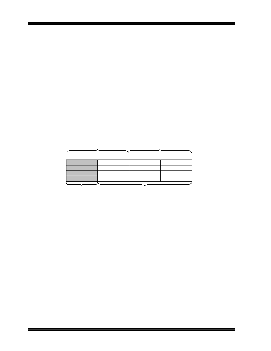
FIGURE 4-2:
PROGRAM MEMORY ORGANIZATION
0
8
16
PC Address
0x000000
0x000002
0x000004
0x000006
23
00000000
Program Memory
‘Phantom’ Byte
(read as ‘0’)
least significant word (lsw)
most significant word (msw)
Instruction Width
0x000001
0x000003
0x000005
0x000007
msw
Address
(lsw Address)
相关PDF资料 |
PDF描述 |
|---|---|
| DSPIC33FJ16GP304-I/ML | IC DSPIC MCU/DSP 16K 44QFN |
| DSPIC33FJ16GS404T-50I/PT | IC MCU/DSP 16KB FLASH 44-TQFP |
| DSPIC33FJ256GP510-I/PF | IC DSPIC MCU/DSP 256K 100TQFP |
| DSPIC33FJ256MC510-I/PF | IC DSPIC MCU/DSP 256K 100TQFP |
| DSPIC33FJ256MC710-I/PF | IC DSPIC MCU/DSP 256K 100TQFP |
相关代理商/技术参数 |
参数描述 |
|---|---|
| dsPIC33FJ12MC202T-E/ML | 功能描述:数字信号处理器和控制器 - DSP, DSC 12KB FLSH 1024BRAM 16B nanoWatt RoHS:否 制造商:Microchip Technology 核心:dsPIC 数据总线宽度:16 bit 程序存储器大小:16 KB 数据 RAM 大小:2 KB 最大时钟频率:40 MHz 可编程输入/输出端数量:35 定时器数量:3 设备每秒兆指令数:50 MIPs 工作电源电压:3.3 V 最大工作温度:+ 85 C 封装 / 箱体:TQFP-44 安装风格:SMD/SMT |
| dsPIC33FJ12MC202T-E/SO | 功能描述:数字信号处理器和控制器 - DSP, DSC 12KB FLSH 1024BRAM 16B nanoWatt RoHS:否 制造商:Microchip Technology 核心:dsPIC 数据总线宽度:16 bit 程序存储器大小:16 KB 数据 RAM 大小:2 KB 最大时钟频率:40 MHz 可编程输入/输出端数量:35 定时器数量:3 设备每秒兆指令数:50 MIPs 工作电源电压:3.3 V 最大工作温度:+ 85 C 封装 / 箱体:TQFP-44 安装风格:SMD/SMT |
| dsPIC33FJ12MC202T-I/ML | 功能描述:数字信号处理器和控制器 - DSP, DSC 12KB FLSH 1024BRAM 16B nanoWatt RoHS:否 制造商:Microchip Technology 核心:dsPIC 数据总线宽度:16 bit 程序存储器大小:16 KB 数据 RAM 大小:2 KB 最大时钟频率:40 MHz 可编程输入/输出端数量:35 定时器数量:3 设备每秒兆指令数:50 MIPs 工作电源电压:3.3 V 最大工作温度:+ 85 C 封装 / 箱体:TQFP-44 安装风格:SMD/SMT |
| dsPIC33FJ12MC202T-I/SO | 功能描述:数字信号处理器和控制器 - DSP, DSC 12KB FLSH 1024BRAM 16B nanoWatt RoHS:否 制造商:Microchip Technology 核心:dsPIC 数据总线宽度:16 bit 程序存储器大小:16 KB 数据 RAM 大小:2 KB 最大时钟频率:40 MHz 可编程输入/输出端数量:35 定时器数量:3 设备每秒兆指令数:50 MIPs 工作电源电压:3.3 V 最大工作温度:+ 85 C 封装 / 箱体:TQFP-44 安装风格:SMD/SMT |
| dsPIC33FJ12MC202T-I/SS | 功能描述:数字信号处理器和控制器 - DSP, DSC 16B Microcontrollers RoHS:否 制造商:Microchip Technology 核心:dsPIC 数据总线宽度:16 bit 程序存储器大小:16 KB 数据 RAM 大小:2 KB 最大时钟频率:40 MHz 可编程输入/输出端数量:35 定时器数量:3 设备每秒兆指令数:50 MIPs 工作电源电压:3.3 V 最大工作温度:+ 85 C 封装 / 箱体:TQFP-44 安装风格:SMD/SMT |
发布紧急采购,3分钟左右您将得到回复。