- 您现在的位置:买卖IC网 > PDF目录1918 > DSPIC33FJ16GS404T-50I/PT (Microchip Technology)IC MCU/DSP 16KB FLASH 44-TQFP PDF资料下载
参数资料
| 型号: | DSPIC33FJ16GS404T-50I/PT |
| 厂商: | Microchip Technology |
| 文件页数: | 157/182页 |
| 文件大小: | 0K |
| 描述: | IC MCU/DSP 16KB FLASH 44-TQFP |
| 标准包装: | 1,200 |
| 系列: | dsPIC™ 33F |
| 核心处理器: | dsPIC |
| 芯体尺寸: | 16-位 |
| 速度: | 50 MIPs |
| 连通性: | I²C,IrDA,LIN,SPI,UART/USART |
| 外围设备: | 欠压检测/复位,POR,PWM,WDT |
| 输入/输出数: | 35 |
| 程序存储器容量: | 16KB(16K x 8) |
| 程序存储器类型: | 闪存 |
| RAM 容量: | 2K x 8 |
| 电压 - 电源 (Vcc/Vdd): | 3 V ~ 3.6 V |
| 数据转换器: | A/D 8x10b |
| 振荡器型: | 内部 |
| 工作温度: | -40°C ~ 85°C |
| 封装/外壳: | 44-TQFP |
| 包装: | 带卷 (TR) |
第1页第2页第3页第4页第5页第6页第7页第8页第9页第10页第11页第12页第13页第14页第15页第16页第17页第18页第19页第20页第21页第22页第23页第24页第25页第26页第27页第28页第29页第30页第31页第32页第33页第34页第35页第36页第37页第38页第39页第40页第41页第42页第43页第44页第45页第46页第47页第48页第49页第50页第51页第52页第53页第54页第55页第56页第57页第58页第59页第60页第61页第62页第63页第64页第65页第66页第67页第68页第69页第70页第71页第72页第73页第74页第75页第76页第77页第78页第79页第80页第81页第82页第83页第84页第85页第86页第87页第88页第89页第90页第91页第92页第93页第94页第95页第96页第97页第98页第99页第100页第101页第102页第103页第104页第105页第106页第107页第108页第109页第110页第111页第112页第113页第114页第115页第116页第117页第118页第119页第120页第121页第122页第123页第124页第125页第126页第127页第128页第129页第130页第131页第132页第133页第134页第135页第136页第137页第138页第139页第140页第141页第142页第143页第144页第145页第146页第147页第148页第149页第150页第151页第152页第153页第154页第155页第156页当前第157页第158页第159页第160页第161页第162页第163页第164页第165页第166页第167页第168页第169页第170页第171页第172页第173页第174页第175页第176页第177页第178页第179页第180页第181页第182页
dsPIC33FJ06GS101/X02 and dsPIC33FJ16GSX02/X04
DS70318F-page 76
2008-2012 Microchip Technology Inc.
4.6
Interfacing Program and Data
Memory Spaces
The dsPIC33FJ06GS101/X02 and dsPIC33FJ16GSX02/
X04 architecture uses a 24-bit-wide program space and a
16-bit-wide data space. The architecture is also a
modified Harvard scheme, meaning that data can also be
present in the program space. To use this data
successfully, it must be accessed in a way that preserves
the alignment of information in both spaces.
Aside from normal execution, the dsPIC33FJ06GS101/
X02
and
dsPIC33FJ16GSX02/X04
architecture
provides two methods by which program space can be
accessed during operation:
Using table instructions to access individual bytes
or words anywhere in the program space
Remapping a portion of the program space into
the data space (Program Space Visibility)
Table instructions allow an application to read or write
to small areas of the program memory. This capability
makes the method ideal for accessing data tables that
need to be updated periodically. It also allows access
to all bytes of the program word. The remapping
method allows an application to access a large block of
data on a read-only basis, which is ideal for look ups
from a large table of static data. The application can
only access the least significant word of the program
word.
4.6.1
ADDRESSING PROGRAM SPACE
Since the address ranges for the data and program
spaces are 16 and 24 bits, respectively, a method is
needed to create a 23-bit or 24-bit program address
from 16-bit data registers. The solution depends on the
interface method to be used.
For table operations, the 8-bit Table Page register
(TBLPAG) is used to define a 32K word region within
the program space. This is concatenated with a 16-bit
EA to arrive at a full 24-bit program space address. In
this format, the Most Significant bit of TBLPAG is used
to determine if the operation occurs in the user memory
(TBLPAG<7> = 0) or the configuration memory
(TBLPAG<7> = 1).
For remapping operations, the 8-bit Program Space
Visibility Register (PSVPAG) is used to define a
16K word page in the program space. When the Most
Significant bit of the EA is ‘1’, PSVPAG is concatenated
with the lower 15 bits of the EA to form a 23-bit program
space address. Unlike table operations, this limits
remapping operations strictly to the user memory area.
Table 4-50 and Figure 4-9 show how the program EA is
created for table operations and remapping accesses
from the data EA. Here, P<23:0> refers to a program
space word, and D<15:0> refers to a data space word.
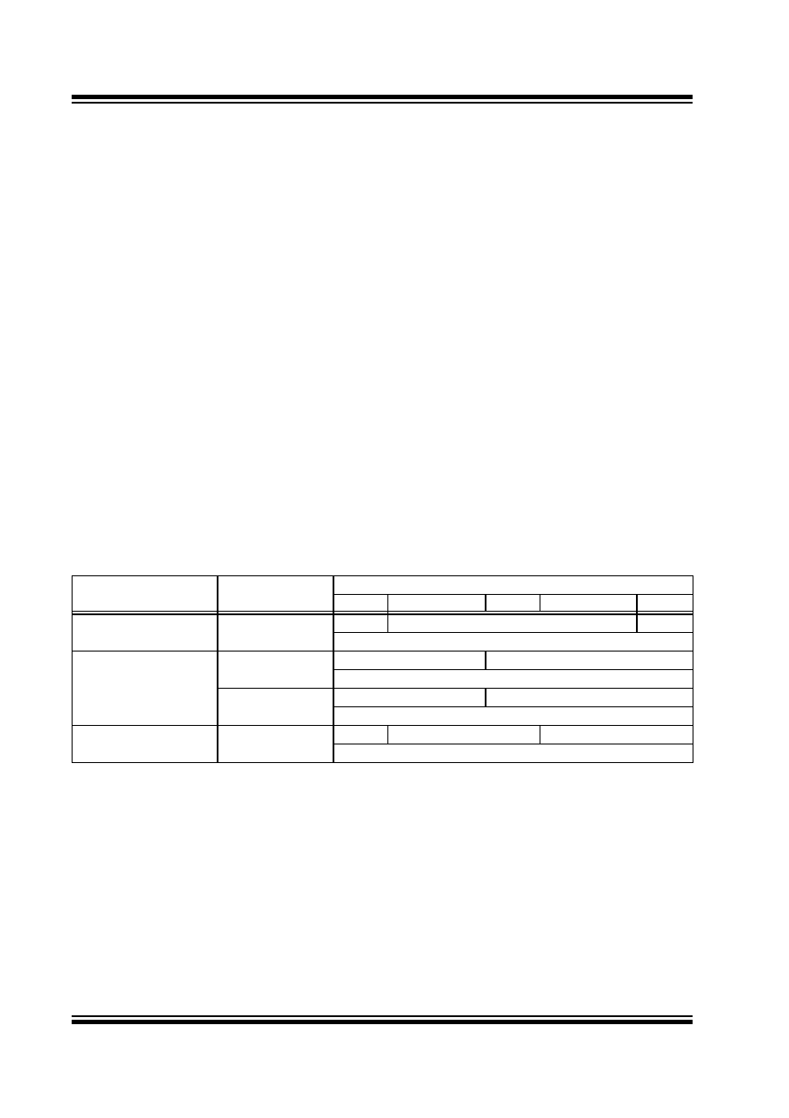
TABLE 4-50:
PROGRAM SPACE ADDRESS CONSTRUCTION
Access Type
Access
Space
Program Space Address
<23>
<22:16>
<15>
<14:1>
<0>
Instruction Access
(Code Execution)
User
0
PC<22:1>
0
0xx xxxx xxxx xxxx xxxx xxx0
TBLRD/TBLWT
(Byte/Word Read/Write)
User
TBLPAG<7:0>
Data EA<15:0>
0xxx xxxx
xxxx xxxx xxxx xxxx
Configuration
TBLPAG<7:0>
Data EA<15:0>
1xxx xxxx
xxxx xxxx xxxx xxxx
Program Space Visibility
(Block Remap/Read)
User
0
PSVPAG<7:0>
Data EA<14:0>(1)
0
xxxx xxxx
xxx xxxx xxxx xxxx
Note 1:
Data EA<15> is always ‘1’ in this case, but is not used in calculating the program space address. Bit 15 of
the address is PSVPAG<0>.
相关PDF资料 |
PDF描述 |
|---|---|
| DSPIC33FJ256GP510-I/PF | IC DSPIC MCU/DSP 256K 100TQFP |
| DSPIC33FJ256MC510-I/PF | IC DSPIC MCU/DSP 256K 100TQFP |
| DSPIC33FJ256MC710-I/PF | IC DSPIC MCU/DSP 256K 100TQFP |
| DSPIC33FJ32MC202-E/MM | IC DSPIC MCU/DSP 32K 28QFN |
| DSPIC33FJ64MC710-I/PF | IC DSPIC MCU/DSP 64K 100TQFP |
相关代理商/技术参数 |
参数描述 |
|---|---|
| dsPIC33FJ16GS404T-E/TL | 功能描述:数字信号处理器和控制器 - DSP, DSC 16Bit MCU/DSP 40MIPS 16 KB FLASH SMPS RoHS:否 制造商:Microchip Technology 核心:dsPIC 数据总线宽度:16 bit 程序存储器大小:16 KB 数据 RAM 大小:2 KB 最大时钟频率:40 MHz 可编程输入/输出端数量:35 定时器数量:3 设备每秒兆指令数:50 MIPs 工作电源电压:3.3 V 最大工作温度:+ 85 C 封装 / 箱体:TQFP-44 安装风格:SMD/SMT |
| dsPIC33FJ16GS404T-I/ML | 功能描述:数字信号处理器和控制器 - DSP, DSC 16B MCU/DSP 44 LD 40MIPS 16 KB FLASH RoHS:否 制造商:Microchip Technology 核心:dsPIC 数据总线宽度:16 bit 程序存储器大小:16 KB 数据 RAM 大小:2 KB 最大时钟频率:40 MHz 可编程输入/输出端数量:35 定时器数量:3 设备每秒兆指令数:50 MIPs 工作电源电压:3.3 V 最大工作温度:+ 85 C 封装 / 箱体:TQFP-44 安装风格:SMD/SMT |
| dsPIC33FJ16GS404T-I/PT | 功能描述:数字信号处理器和控制器 - DSP, DSC 16B MCU/DSP 40MIPS 16 KB FLASH RoHS:否 制造商:Microchip Technology 核心:dsPIC 数据总线宽度:16 bit 程序存储器大小:16 KB 数据 RAM 大小:2 KB 最大时钟频率:40 MHz 可编程输入/输出端数量:35 定时器数量:3 设备每秒兆指令数:50 MIPs 工作电源电压:3.3 V 最大工作温度:+ 85 C 封装 / 箱体:TQFP-44 安装风格:SMD/SMT |
| dsPIC33FJ16GS404T-I/TL | 功能描述:数字信号处理器和控制器 - DSP, DSC 16Bit MCU/DSP 40MIPS 16 KB FLASH SMPS RoHS:否 制造商:Microchip Technology 核心:dsPIC 数据总线宽度:16 bit 程序存储器大小:16 KB 数据 RAM 大小:2 KB 最大时钟频率:40 MHz 可编程输入/输出端数量:35 定时器数量:3 设备每秒兆指令数:50 MIPs 工作电源电压:3.3 V 最大工作温度:+ 85 C 封装 / 箱体:TQFP-44 安装风格:SMD/SMT |
| dsPIC33FJ16GS502-50I/MM | 功能描述:数字信号处理器和控制器 - DSP, DSC 16B MCU/DSP 50MIPS 16KB FL SMPS RoHS:否 制造商:Microchip Technology 核心:dsPIC 数据总线宽度:16 bit 程序存储器大小:16 KB 数据 RAM 大小:2 KB 最大时钟频率:40 MHz 可编程输入/输出端数量:35 定时器数量:3 设备每秒兆指令数:50 MIPs 工作电源电压:3.3 V 最大工作温度:+ 85 C 封装 / 箱体:TQFP-44 安装风格:SMD/SMT |
发布紧急采购,3分钟左右您将得到回复。