- 您现在的位置:买卖IC网 > PDF目录3851 > DSPIC33FJ32GP202-I/SO (Microchip Technology)IC DSPIC MCU/DSP 32K 28SOIC PDF资料下载
参数资料
| 型号: | DSPIC33FJ32GP202-I/SO |
| 厂商: | Microchip Technology |
| 文件页数: | 64/176页 |
| 文件大小: | 0K |
| 描述: | IC DSPIC MCU/DSP 32K 28SOIC |
| 产品培训模块: | Asynchronous Stimulus |
| 特色产品: | PIC24FJ/33FJ MCUs & dsPIC? DSCs |
| 标准包装: | 27 |
| 系列: | dsPIC™ 33F |
| 核心处理器: | dsPIC |
| 芯体尺寸: | 16-位 |
| 速度: | 40 MIP |
| 连通性: | I²C,IrDA,LIN,SPI,UART/USART |
| 外围设备: | 欠压检测/复位,POR,PWM,WDT |
| 输入/输出数: | 21 |
| 程序存储器容量: | 32KB(32K x 8) |
| 程序存储器类型: | 闪存 |
| RAM 容量: | 2K x 8 |
| 电压 - 电源 (Vcc/Vdd): | 3 V ~ 3.6 V |
| 数据转换器: | A/D 10x12b |
| 振荡器型: | 内部 |
| 工作温度: | -40°C ~ 85°C |
| 封装/外壳: | 28-SOIC(0.295",7.50mm 宽) |
| 包装: | 管件 |
| 产品目录页面: | 652 (CN2011-ZH PDF) |
| 配用: | DV164033-ND - KIT START EXPLORER 16 MPLAB ICD2 DM240001-ND - BOARD DEMO PIC24/DSPIC33/PIC32 |
第1页第2页第3页第4页第5页第6页第7页第8页第9页第10页第11页第12页第13页第14页第15页第16页第17页第18页第19页第20页第21页第22页第23页第24页第25页第26页第27页第28页第29页第30页第31页第32页第33页第34页第35页第36页第37页第38页第39页第40页第41页第42页第43页第44页第45页第46页第47页第48页第49页第50页第51页第52页第53页第54页第55页第56页第57页第58页第59页第60页第61页第62页第63页当前第64页第65页第66页第67页第68页第69页第70页第71页第72页第73页第74页第75页第76页第77页第78页第79页第80页第81页第82页第83页第84页第85页第86页第87页第88页第89页第90页第91页第92页第93页第94页第95页第96页第97页第98页第99页第100页第101页第102页第103页第104页第105页第106页第107页第108页第109页第110页第111页第112页第113页第114页第115页第116页第117页第118页第119页第120页第121页第122页第123页第124页第125页第126页第127页第128页第129页第130页第131页第132页第133页第134页第135页第136页第137页第138页第139页第140页第141页第142页第143页第144页第145页第146页第147页第148页第149页第150页第151页第152页第153页第154页第155页第156页第157页第158页第159页第160页第161页第162页第163页第164页第165页第166页第167页第168页第169页第170页第171页第172页第173页第174页第175页第176页
154
AT89C5131
4136C–USB–04/05
Notes:
1. Operating I
CC is measured with all output pins disconnected; XTAL1 driven with TCLCH, TCHCL = 5 ns (see Figure 73.), VIL =
V
SS + 0.5V,
VIH = VCC - 0.5V; XTAL2 N.C.; EA = RST = Port 0 = VCC. ICC would be slightly higher if a crystal oscillator used (see Figure
70.).
2. Idle I
CC is measured with all output pins disconnected; XTAL1 driven with TCLCH, TCHCL = 5 ns, VIL = VSS + 0.5V, VIH = VCC -
0.5V; XTAL2 N.C; Port 0 = V
3. Power-down I
CC is measured with all output pins disconnected; EA = VCC, PORT 0 = VCC; XTAL2 NC.; RST = VSS (see Fig-
ure 72.). In addition, the WDT must be inactive and the POF flag must be set.
4. Capacitance loading on Ports 0 and 2 may cause spurious noise pulses to be superimposed on the V
OLS of ALE and Ports 1
and 3. The noise is due to external bus capacitance discharging into the Port 0 and Port 2 pins when these pins make 1 to 0
transitions during bus operation. In the worst cases (capacitive loading 100 pF), the noise pulse on the ALE line may exceed
0.45V with maxi V
OL peak 0.6V. A Schmitt Trigger use is not necessary.
5. Typicals are based on a limited number of samples and are not guaranteed. The values listed are at room temperature.
6. Under steady state (non-transient) conditions, I
OL must be externally limited as follows:
Maximum I
OL per port pin: 10 mA
Maximum I
OL per 8-bit port:
Port 0: 26 mA
Ports 1, 2 and 3: 15 mA
Maximum total I
OL for all output pins: 71 mA
If I
OL exceeds the test condition, VOL may exceed the related specification. Pins are not guaranteed to sink current greater
than the listed test conditions.
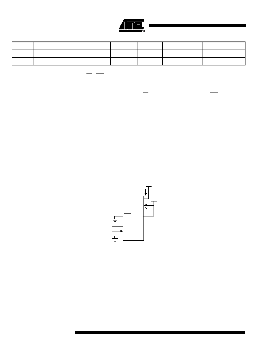
Figure 70. I
CC Test Condition, Active Mode
V
PFDM
Power Fail Low Level Threshold
2.2
V
Power fail hysteresis V
PFDP - VPFDM
0.15
V
Symbol
Parameter
Min
Typ
(5)
Max
Unit
Test Conditions
EA
V
CC
VCC
I
CC
(NC)
CLOCK
SIGNAL
All other pins are disconnected.
RST
XTAL2
XTAL1
VSS
VCC
P0
相关PDF资料 |
PDF描述 |
|---|---|
| PIC18LF27J13-I/ML | IC PIC MCU 128KB FLASH 28QFN |
| PIC24FJ64GA006-I/MR | MCU 64KB FLASH 8KB RAM 64-QFN |
| DSPIC30F2010-20I/MM | IC DSPIC MCU/DSP 12K 28QFN |
| PIC32MX150F128B-I/SO | IC MCU 32BIT 128KB FLASH 28-SOIC |
| PIC32MX230F064B-I/SO | IC MCU 32BIT 64KB FLASH 28-SOIC |
相关代理商/技术参数 |
参数描述 |
|---|---|
| DSPIC33FJ32GP202T-E/MM | 制造商:Microchip Technology Inc 功能描述: |
| dsPIC33FJ32GP202T-I/MM | 功能描述:数字信号处理器和控制器 - DSP, DSC 16B DSC 28LD32KB 40 MIPS RoHS:否 制造商:Microchip Technology 核心:dsPIC 数据总线宽度:16 bit 程序存储器大小:16 KB 数据 RAM 大小:2 KB 最大时钟频率:40 MHz 可编程输入/输出端数量:35 定时器数量:3 设备每秒兆指令数:50 MIPs 工作电源电压:3.3 V 最大工作温度:+ 85 C 封装 / 箱体:TQFP-44 安装风格:SMD/SMT |
| dsPIC33FJ32GP202T-I/SO | 功能描述:数字信号处理器和控制器 - DSP, DSC 16B DSC 28LD32KB 40 MIPS RoHS:否 制造商:Microchip Technology 核心:dsPIC 数据总线宽度:16 bit 程序存储器大小:16 KB 数据 RAM 大小:2 KB 最大时钟频率:40 MHz 可编程输入/输出端数量:35 定时器数量:3 设备每秒兆指令数:50 MIPs 工作电源电压:3.3 V 最大工作温度:+ 85 C 封装 / 箱体:TQFP-44 安装风格:SMD/SMT |
| dsPIC33FJ32GP202T-I/SS | 功能描述:数字信号处理器和控制器 - DSP, DSC 16 bit DSC 40MIPS 32KB Flash RoHS:否 制造商:Microchip Technology 核心:dsPIC 数据总线宽度:16 bit 程序存储器大小:16 KB 数据 RAM 大小:2 KB 最大时钟频率:40 MHz 可编程输入/输出端数量:35 定时器数量:3 设备每秒兆指令数:50 MIPs 工作电源电压:3.3 V 最大工作温度:+ 85 C 封装 / 箱体:TQFP-44 安装风格:SMD/SMT |
| dsPIC33FJ32GP204-E/ML | 功能描述:数字信号处理器和控制器 - DSP, DSC 16B DSC 44LD32KB 40 MIPS RoHS:否 制造商:Microchip Technology 核心:dsPIC 数据总线宽度:16 bit 程序存储器大小:16 KB 数据 RAM 大小:2 KB 最大时钟频率:40 MHz 可编程输入/输出端数量:35 定时器数量:3 设备每秒兆指令数:50 MIPs 工作电源电压:3.3 V 最大工作温度:+ 85 C 封装 / 箱体:TQFP-44 安装风格:SMD/SMT |
发布紧急采购,3分钟左右您将得到回复。