- 您现在的位置:买卖IC网 > PDF目录3843 > DSPIC33FJ32MC204-I/ML (Microchip Technology)IC DSPIC MCU/DSP 32K 44QFN PDF资料下载
参数资料
| 型号: | DSPIC33FJ32MC204-I/ML |
| 厂商: | Microchip Technology |
| 文件页数: | 47/76页 |
| 文件大小: | 0K |
| 描述: | IC DSPIC MCU/DSP 32K 44QFN |
| 产品培训模块: | Asynchronous Stimulus |
| 特色产品: | PIC24FJ/33FJ MCUs & dsPIC? DSCs |
| 标准包装: | 45 |
| 系列: | dsPIC™ 33F |
| 核心处理器: | dsPIC |
| 芯体尺寸: | 16-位 |
| 速度: | 40 MIP |
| 连通性: | I²C,IrDA,LIN,SPI,UART/USART |
| 外围设备: | 欠压检测/复位,DMA,电机控制 PWM,QEI,POR,PWM,WDT |
| 输入/输出数: | 35 |
| 程序存储器容量: | 32KB(32K x 8) |
| 程序存储器类型: | 闪存 |
| RAM 容量: | 2K x 8 |
| 电压 - 电源 (Vcc/Vdd): | 3 V ~ 3.6 V |
| 数据转换器: | A/D 9x10b/12b |
| 振荡器型: | 内部 |
| 工作温度: | -40°C ~ 85°C |
| 封装/外壳: | 44-VQFN 裸露焊盘 |
| 包装: | 管件 |
| 产品目录页面: | 652 (CN2011-ZH PDF) |
| 配用: | DV164033-ND - KIT START EXPLORER 16 MPLAB ICD2 DM240001-ND - BOARD DEMO PIC24/DSPIC33/PIC32 |
第1页第2页第3页第4页第5页第6页第7页第8页第9页第10页第11页第12页第13页第14页第15页第16页第17页第18页第19页第20页第21页第22页第23页第24页第25页第26页第27页第28页第29页第30页第31页第32页第33页第34页第35页第36页第37页第38页第39页第40页第41页第42页第43页第44页第45页第46页当前第47页第48页第49页第50页第51页第52页第53页第54页第55页第56页第57页第58页第59页第60页第61页第62页第63页第64页第65页第66页第67页第68页第69页第70页第71页第72页第73页第74页第75页第76页
2007-2012 Microchip Technology Inc.
DS70283K-page 51
dsPIC33FJ32MC202/204 and dsPIC33FJ16MC304
4.8
Interfacing Program and Data
Memory Spaces
The
dsPIC33FJ32MC202/204
and
dsPIC33FJ16MC304 architecture uses a 24-bit-wide
program space and a 16-bit-wide data space. The
architecture is also a modified Harvard scheme,
meaning that data can also be present in the program
space. To use this data successfully, it must be
accessed in a way that preserves the alignment of
information in both spaces.
Aside
from
normal
execution,
the
dsPIC33FJ32MC202/204 and dsPIC33FJ16MC304
architecture provides two methods by which program
space can be accessed during operation:
Using table instructions to access individual bytes
or words anywhere in the program space
Remapping a portion of the program space into
the data space (Program Space Visibility)
Table instructions allow an application to read or write
to small areas of the program memory. This capability
makes the method ideal for accessing data tables that
need to be updated periodically. It also allows access
to all bytes of the program word. The remapping
method allows an application to access a large block of
data on a read-only basis, which is ideal for look-ups
from a large table of static data. The application can
only access the least significant word of the program
word.
4.8.1
ADDRESSING PROGRAM SPACE
Since the address ranges for the data and program
spaces are 16 and 24 bits, respectively, a method is
needed to create a 23-bit or 24-bit program address
from 16-bit data registers. The solution depends on the
interface method to be used.
For table operations, the 8-bit Table Page register
(TBLPAG) is used to define a 32K word region within
the program space. This is concatenated with a 16-bit
EA to arrive at a full 24-bit program space address. In
this format, the Most Significant bit of TBLPAG is used
to determine if the operation occurs in the user memory
(TBLPAG<7> = 0) or the configuration memory
(TBLPAG<7> = 1).
For remapping operations, the 8-bit Program Space
Visibility register (PSVPAG) is used to define a
16K word page in the program space. When the Most
Significant bit of the EA is ‘1’, PSVPAG is concatenated
with the lower 15 bits of the EA to form a 23-bit program
space address. Unlike table operations, this limits
remapping operations strictly to the user memory area.
Table 4-28 and Figure 4-7 show how the program EA is
created for table operations and remapping accesses
from the data EA. Here, P<23:0> refers to a program
space word, and D<15:0> refers to a data space word.
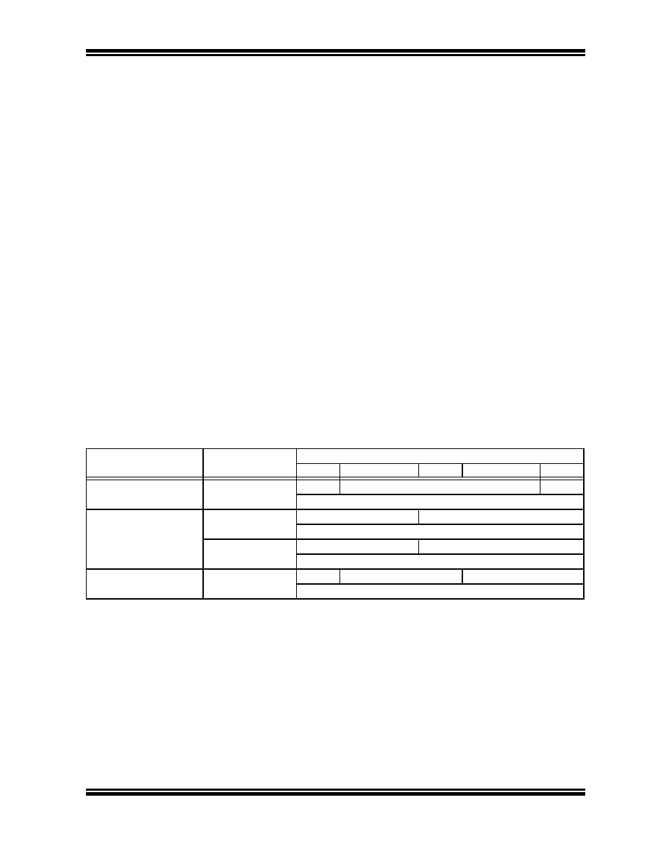
TABLE 4-28:
PROGRAM SPACE ADDRESS CONSTRUCTION
Access Type
Access
Space
Program Space Address
<23>
<22:16>
<15>
<14:1>
<0>
Instruction Access
(Code Execution)
User
0
PC<22:1>
0
0xx
xxxx
xxxx xxx0
TBLRD/TBLWT
(Byte/Word Read/Write)
User
TBLPAG<7:0>
Data EA<15:0>
0xxx xxxx
xxxx xxxx xxxx xxxx
Configuration
TBLPAG<7:0>
Data EA<15:0>
1xxx xxxx
xxxx xxxx xxxx xxxx
Program Space Visibility
(Block Remap/Read)
User
0
PSVPAG<7:0>
Data EA<14:0>(1)
0
xxxx xxxx
xxx xxxx xxxx xxxx
Note 1: Data EA<15> is always ‘1’ in this case, but is not used in calculating the program space address. Bit 15 of
the address is PSVPAG<0>.
相关PDF资料 |
PDF描述 |
|---|---|
| TS87C51RC2-VIA | IC MCU 8BIT 32K OTP 40MHZ 40-DIP |
| TS87C51RD2-VCA | IC MCU 8BIT 64K OTP 40MHZ 40-DIP |
| 52610-1690 | CONN FFC/FPC 16POS 1MM VERT SMD |
| TSC80251G2D-L16CB | IC MCU 8BIT 16MHZ LO VOLT 44PLCC |
| TSC87251G2D-16CB | IC MCU 8BIT 32K OTP 16MHZ 44PLCC |
相关代理商/技术参数 |
参数描述 |
|---|---|
| dsPIC33FJ32MC204T-I/ML | 功能描述:数字信号处理器和控制器 - DSP, DSC 16B DSC 44LD32KB Motor40 MIPS RoHS:否 制造商:Microchip Technology 核心:dsPIC 数据总线宽度:16 bit 程序存储器大小:16 KB 数据 RAM 大小:2 KB 最大时钟频率:40 MHz 可编程输入/输出端数量:35 定时器数量:3 设备每秒兆指令数:50 MIPs 工作电源电压:3.3 V 最大工作温度:+ 85 C 封装 / 箱体:TQFP-44 安装风格:SMD/SMT |
| dsPIC33FJ32MC204T-I/PT | 功能描述:数字信号处理器和控制器 - DSP, DSC 16B DSC 32KB Motor40 MIPS RoHS:否 制造商:Microchip Technology 核心:dsPIC 数据总线宽度:16 bit 程序存储器大小:16 KB 数据 RAM 大小:2 KB 最大时钟频率:40 MHz 可编程输入/输出端数量:35 定时器数量:3 设备每秒兆指令数:50 MIPs 工作电源电压:3.3 V 最大工作温度:+ 85 C 封装 / 箱体:TQFP-44 安装风格:SMD/SMT |
| dsPIC33FJ32MC302-E/MM | 功能描述:数字信号处理器和控制器 - DSP, DSC 16B MCU/DSP 28 LD 40MIPS 32 KB FLASH RoHS:否 制造商:Microchip Technology 核心:dsPIC 数据总线宽度:16 bit 程序存储器大小:16 KB 数据 RAM 大小:2 KB 最大时钟频率:40 MHz 可编程输入/输出端数量:35 定时器数量:3 设备每秒兆指令数:50 MIPs 工作电源电压:3.3 V 最大工作温度:+ 85 C 封装 / 箱体:TQFP-44 安装风格:SMD/SMT |
| dsPIC33FJ32MC302-E/SO | 功能描述:数字信号处理器和控制器 - DSP, DSC 16B DSC 28LD32KB DMA 40MIPS RoHS:否 制造商:Microchip Technology 核心:dsPIC 数据总线宽度:16 bit 程序存储器大小:16 KB 数据 RAM 大小:2 KB 最大时钟频率:40 MHz 可编程输入/输出端数量:35 定时器数量:3 设备每秒兆指令数:50 MIPs 工作电源电压:3.3 V 最大工作温度:+ 85 C 封装 / 箱体:TQFP-44 安装风格:SMD/SMT |
| dsPIC33FJ32MC302-E/SP | 功能描述:数字信号处理器和控制器 - DSP, DSC 16B DSC 28LD32KB DMA 40MIPS RoHS:否 制造商:Microchip Technology 核心:dsPIC 数据总线宽度:16 bit 程序存储器大小:16 KB 数据 RAM 大小:2 KB 最大时钟频率:40 MHz 可编程输入/输出端数量:35 定时器数量:3 设备每秒兆指令数:50 MIPs 工作电源电压:3.3 V 最大工作温度:+ 85 C 封装 / 箱体:TQFP-44 安装风格:SMD/SMT |
发布紧急采购,3分钟左右您将得到回复。