- 您现在的位置:买卖IC网 > PDF目录3869 > DSPIC33FJ64MC710T-I/PF (Microchip Technology)IC DSPIC MCU/DSP 64K 100TQFP PDF资料下载
参数资料
| 型号: | DSPIC33FJ64MC710T-I/PF |
| 厂商: | Microchip Technology |
| 文件页数: | 174/199页 |
| 文件大小: | 0K |
| 描述: | IC DSPIC MCU/DSP 64K 100TQFP |
| 产品培训模块: | Asynchronous Stimulus |
| 标准包装: | 1,000 |
| 系列: | dsPIC™ 33F |
| 核心处理器: | dsPIC |
| 芯体尺寸: | 16-位 |
| 速度: | 40 MIP |
| 连通性: | CAN,I²C,IrDA,LIN,SPI,UART/USART |
| 外围设备: | 欠压检测/复位,DMA,电机控制 PWM,QEI,POR,PWM,WDT |
| 输入/输出数: | 85 |
| 程序存储器容量: | 64KB(64K x 8) |
| 程序存储器类型: | 闪存 |
| RAM 容量: | 16K x 8 |
| 电压 - 电源 (Vcc/Vdd): | 3 V ~ 3.6 V |
| 数据转换器: | A/D 24x10b/12b |
| 振荡器型: | 内部 |
| 工作温度: | -40°C ~ 85°C |
| 封装/外壳: | 100-TQFP |
| 包装: | 带卷 (TR) |
| 配用: | MA330013-ND - MODULE PLUG-IN DSPIC33 100TQFP DV164033-ND - KIT START EXPLORER 16 MPLAB ICD2 DM240001-ND - BOARD DEMO PIC24/DSPIC33/PIC32 AC164323-ND - MODULE SKT FOR 100TQFP |
第1页第2页第3页第4页第5页第6页第7页第8页第9页第10页第11页第12页第13页第14页第15页第16页第17页第18页第19页第20页第21页第22页第23页第24页第25页第26页第27页第28页第29页第30页第31页第32页第33页第34页第35页第36页第37页第38页第39页第40页第41页第42页第43页第44页第45页第46页第47页第48页第49页第50页第51页第52页第53页第54页第55页第56页第57页第58页第59页第60页第61页第62页第63页第64页第65页第66页第67页第68页第69页第70页第71页第72页第73页第74页第75页第76页第77页第78页第79页第80页第81页第82页第83页第84页第85页第86页第87页第88页第89页第90页第91页第92页第93页第94页第95页第96页第97页第98页第99页第100页第101页第102页第103页第104页第105页第106页第107页第108页第109页第110页第111页第112页第113页第114页第115页第116页第117页第118页第119页第120页第121页第122页第123页第124页第125页第126页第127页第128页第129页第130页第131页第132页第133页第134页第135页第136页第137页第138页第139页第140页第141页第142页第143页第144页第145页第146页第147页第148页第149页第150页第151页第152页第153页第154页第155页第156页第157页第158页第159页第160页第161页第162页第163页第164页第165页第166页第167页第168页第169页第170页第171页第172页第173页当前第174页第175页第176页第177页第178页第179页第180页第181页第182页第183页第184页第185页第186页第187页第188页第189页第190页第191页第192页第193页第194页第195页第196页第197页第198页第199页
dsPIC33F
DS70165E-page 74
Preliminary
2007 Microchip Technology Inc.
3.6.2
DATA ACCESS FROM PROGRAM
MEMORY USING TABLE
INSTRUCTIONS
The TBLRDL and TBLWTL instructions offer a direct
method of reading or writing the lower word of any
address within the program space without going
through data space. The TBLRDH and TBLWTH instruc-
tions are the only method to read or write the upper
8 bits of a program space word as data.
The PC is incremented by two for each successive
24-bit program word. This allows program memory
addresses to directly map to data space addresses.
Program memory can thus be regarded as two 16-bit
word wide address spaces, residing side by side, each
with the same address range. TBLRDL and TBLWTL
access the space which contains the least significant
data word and TBLRDH and TBLWTH access the space
which contains the upper data byte.
Two table instructions are provided to move byte or
word sized (16-bit) data to and from program space.
Both function as either byte or word operations.
1.
TBLRDL
(Table Read Low): In Word mode, it
maps the lower word of the program space
location (P<15:0>) to a data address (D<15:0>).
In Byte mode, either the upper or lower byte of
the lower program word is mapped to the lower
byte of a data address. The upper byte is
selected when Byte Select is ‘1’; the lower byte
is selected when it is ‘0’.
2.
TBLRDH
(
Table Read High): In Word mode, it
maps the entire upper word of a program address
(P<23:16>) to a data address. Note that
D<15:8>, the ‘phantom byte’, will always be ‘0’.
In Byte mode, it maps the upper or lower byte of
the program word to D<7:0> of the data
address, as above. Note that the data will
always be ‘0’ when the upper ‘phantom’ byte is
selected (Byte Select = 1).
In a similar fashion, two table instructions, TBLWTH
and TBLWTL, are used to write individual bytes or
words to a program space address. The details of
their operation are explained in Section 4.0 “Flash
For all table operations, the area of program memory
space to be accessed is determined by the Table Page
register (TBLPAG). TBLPAG covers the entire program
memory space of the device, including user and config-
uration spaces. When TBLPAG<7> = 0, the table page
is
located
in
the
user
memory
space.
When
TBLPAG<7> = 1, the page is located in configuration
space.
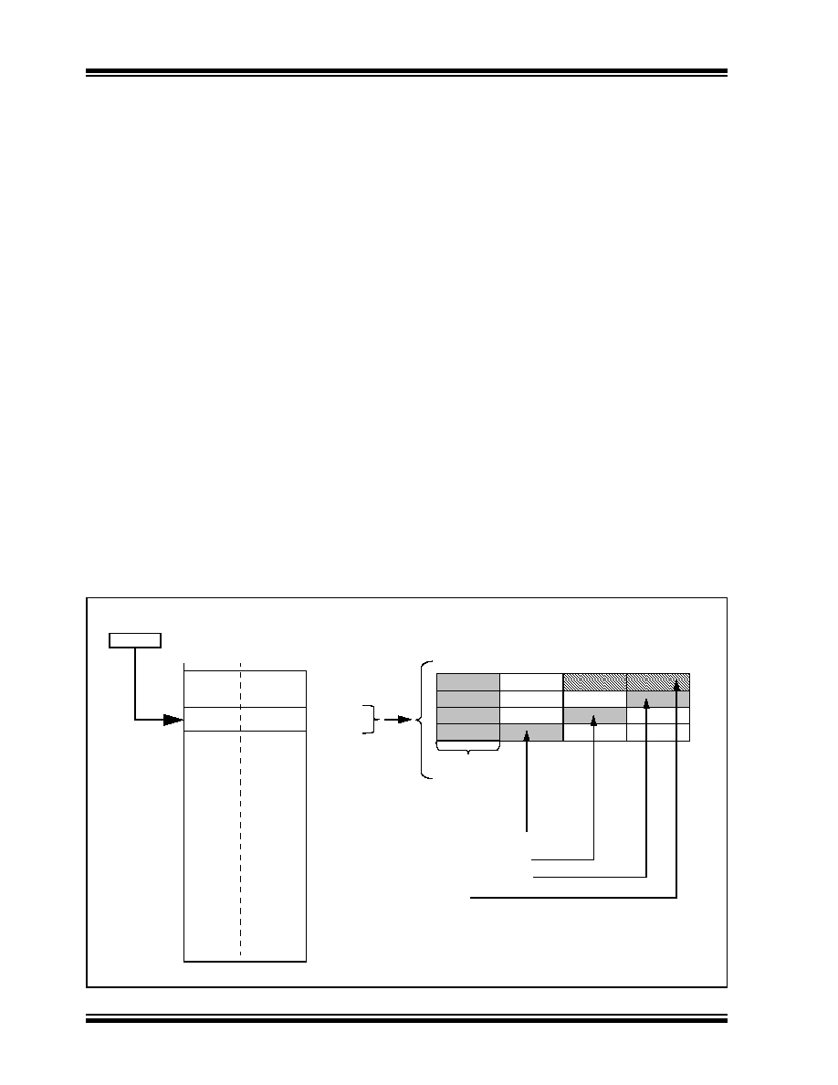
FIGURE 3-10:
ACCESSING PROGRAM MEMORY WITH TABLE INSTRUCTIONS
0
8
16
23
00000000
‘Phantom’ Byte
TBLRDH.B
(Wn<0> = 0)
TBLRDL.W
TBLRDL.B
(Wn<0> = 1)
TBLRDL.B
(Wn<0> = 0)
23
15
0
TBLPAG
02
0x000000
0x800000
0x020000
0x030000
Program Space
The address for the table operation is determined by the data EA
within the page defined by the TBLPAG register.
Only read operations are shown; write operations are also valid in
the user memory area.
相关PDF资料 |
PDF描述 |
|---|---|
| PIC18F66J93-I/PT | IC PIC MCU FLASH 64KX4 64-TQFP |
| DSPIC33FJ64MC510T-I/PT | IC DSPIC MCU/DSP 64K 100TQFP |
| DSPIC33FJ64MC510T-I/PF | IC DSPIC MCU/DSP 64K 100TQFP |
| DSPIC33FJ64GP710T-I/PT | IC DSPIC MCU/DSP 64K 100TQFP |
| DSPIC33FJ64GP710T-I/PF | IC DSPIC MCU/DSP 64K 100TQFP |
相关代理商/技术参数 |
参数描述 |
|---|---|
| dsPIC33FJ64MC802-E/MM | 功能描述:数字信号处理器和控制器 - DSP, DSC 16Bit MCU/DSP 40MIPS 64KB FLASH RoHS:否 制造商:Microchip Technology 核心:dsPIC 数据总线宽度:16 bit 程序存储器大小:16 KB 数据 RAM 大小:2 KB 最大时钟频率:40 MHz 可编程输入/输出端数量:35 定时器数量:3 设备每秒兆指令数:50 MIPs 工作电源电压:3.3 V 最大工作温度:+ 85 C 封装 / 箱体:TQFP-44 安装风格:SMD/SMT |
| dsPIC33FJ64MC802-E/SO | 功能描述:数字信号处理器和控制器 - DSP, DSC 16B DSC 28LD64KB RoHS:否 制造商:Microchip Technology 核心:dsPIC 数据总线宽度:16 bit 程序存储器大小:16 KB 数据 RAM 大小:2 KB 最大时钟频率:40 MHz 可编程输入/输出端数量:35 定时器数量:3 设备每秒兆指令数:50 MIPs 工作电源电压:3.3 V 最大工作温度:+ 85 C 封装 / 箱体:TQFP-44 安装风格:SMD/SMT |
| dsPIC33FJ64MC802-E/SP | 功能描述:数字信号处理器和控制器 - DSP, DSC 16B DSC 28LD64KB RoHS:否 制造商:Microchip Technology 核心:dsPIC 数据总线宽度:16 bit 程序存储器大小:16 KB 数据 RAM 大小:2 KB 最大时钟频率:40 MHz 可编程输入/输出端数量:35 定时器数量:3 设备每秒兆指令数:50 MIPs 工作电源电压:3.3 V 最大工作温度:+ 85 C 封装 / 箱体:TQFP-44 安装风格:SMD/SMT |
| dsPIC33FJ64MC802-H/MM | 功能描述:数字信号处理器和控制器 - DSP, DSC 16-bit 64KB Flash Motor CAN DMA RoHS:否 制造商:Microchip Technology 核心:dsPIC 数据总线宽度:16 bit 程序存储器大小:16 KB 数据 RAM 大小:2 KB 最大时钟频率:40 MHz 可编程输入/输出端数量:35 定时器数量:3 设备每秒兆指令数:50 MIPs 工作电源电压:3.3 V 最大工作温度:+ 85 C 封装 / 箱体:TQFP-44 安装风格:SMD/SMT |
| dsPIC33FJ64MC802-H/SO | 功能描述:数字信号处理器和控制器 - DSP, DSC 16-bit 64KB Flash Motor CAN DMA RoHS:否 制造商:Microchip Technology 核心:dsPIC 数据总线宽度:16 bit 程序存储器大小:16 KB 数据 RAM 大小:2 KB 最大时钟频率:40 MHz 可编程输入/输出端数量:35 定时器数量:3 设备每秒兆指令数:50 MIPs 工作电源电压:3.3 V 最大工作温度:+ 85 C 封装 / 箱体:TQFP-44 安装风格:SMD/SMT |
发布紧急采购,3分钟左右您将得到回复。