- 您现在的位置:买卖IC网 > PDF目录97873 > E672-EDGE672 500 MHz Pin Electronics Window Comparator and Load PDF资料下载
参数资料
| 型号: | E672-EDGE672 |
| 英文描述: | 500 MHz Pin Electronics Window Comparator and Load |
| 中文描述: | 500兆赫引脚电子窗口比较器和负载 |
| 文件页数: | 10/15页 |
| 文件大小: | 118K |
| 代理商: | E672-EDGE672 |
4
2000 Semtech Corp.
www.semtech.com
EDGE HIGH-PERFORMANCE PRODUCTS
Edge672
PRELIMINARY
Circuit Description
Load
Introduction
The load section is capable of sourcing and sinking up
to 35 mA, both statically and dynamically, or being placed
in a high impedance state.
Load Enable
The load is controlled by the load enable input (LDEN /
LDEN*). If LDEN is more positive than LDEN*, the output
diode bridge will be active. If LDEN is more negative
than LDEN*, the LOAD pin will be placed in a high
impedance state.
Source and Sink Levels
The amount of current that the diode bridge can source
and sink is adjustable from 0 mA to 35 mA. The source
and sink levels are separate and independent.
ISCIN is a current input node which programs the bridge
source current. There is a gain of 40 between the ISCIN
current and the bridge source current. ISKIN is a current
input node that programs the bridge sink current. There
is a gain of –40 between the ISKIN current and the bridge
sink current.
ISOURCE = 40 * ISCIN
ISINK = –40 * ISKIN
Caution: The ISKIN and ISCIN inputs are designed for
positive current between 0 mA and .875 mA flowing into
the Edge672. Care should be taken to insure that current
is never required to flow out of the Edge672 on these two
nodes.
Figure 3. Commutating Voltage Compensation
Commutating Voltage
VCMIN is a high input impedance voltage input node
that sets the voltage level at which the diode bridge
switches from sourcing to sinking currents. If LOAD is
more positive than VCMIN, the bridge will sink current
from the DUT into the Edge672 (see Figure 1). If LOAD
is more negative than VCMIN, the bridge will source
current from the Edge672 into the DUT (see Figure 2).
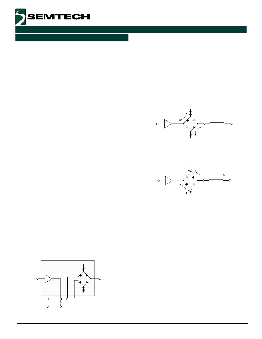
Figure 1. LOAD > VCMIN
The Edge 672 sinks DUT current.
Figure 2. LOAD < VCMIN
The Edge 672 sources DUT current.
Commutating Voltage Compensation
The VCMOUT pin is the actual commutation voltage seen
by the load diode bridge (see Figure 3).
This node
requires a fixed .01
F capacitor (with good high
frequency characteristics) to ground.
The VCMCOMP pin is an analog output pin that requires
a fixed .01
F chip capacitor (with good high frequency
characteristics) to ground (See Figure 3). This capacitor
is used to compensate an internal node on the on-chip
op amp used to buffer the commutating voltage input.
VCMCOMP
VCMIN
VCMOUT
BRIDGE
SINK
BRIDGE
SOURCE
LOAD
.01
F
.01
F
VCMIN
DUT
LOAD
ISOURCE
ISINK
VCMIN
DUT
LOAD
ISOURCE
ISINK
相关PDF资料 |
PDF描述 |
|---|---|
| E692-EDGE692 | 200 MHz Monolithic Dual Pin Electronics Driver |
| E693-EDGE693 | 500 MHz Monolithic Dual Pin Electronics Driver |
| E710-EDGE710 | 500 MHz Pin Electronics Driver. Window Comparator. and Load |
| E720-EDGE720 | 500 MHz Pin Electronics Driver. Window Comparator. and Load |
| E728-EDGE728 | Very High-Speed Dual- and Quad-Channel ECL Delay Lines |
相关代理商/技术参数 |
参数描述 |
|---|---|
| E67312-000 | 制造商:TE Connectivity 功能描述:DK-602-0187-6 - Bulk |
| E-673254-3-9 | 制造商:MA-COM 制造商全称:M/A-COM Technology Solutions, Inc. 功能描述:Label format - Old format order code cross reference |
| E-673349-3-9 | 制造商:TE Connectivity 功能描述:Labels Dot Matrix Printable Label Polyester White 67.3x34.9mm |
| E67377-000 | 制造商:TE Connectivity 功能描述:Shrink Boot Adapters 180 制造商:TE Connectivity 功能描述:TXR54AB00-1810AI2J - Bulk |
| E67401-000 | 制造商:TE Connectivity 功能描述:MP-445445-2-8A - Bulk 制造商:TE Connectivity 功能描述:LABEL ID PRODUCT 制造商:TE Connectivity 功能描述:Labels Thermal Transfer Printable Label Polyester Matte Silver 44.5x44.5mm |
发布紧急采购,3分钟左右您将得到回复。