- 您现在的位置:买卖IC网 > PDF目录97873 > E720-EDGE720 500 MHz Pin Electronics Driver. Window Comparator. and Load PDF资料下载
参数资料
| 型号: | E720-EDGE720 |
| 英文描述: | 500 MHz Pin Electronics Driver. Window Comparator. and Load |
| 中文描述: | 500兆赫引脚电子驱动器。窗口比较器。和负载 |
| 文件页数: | 7/31页 |
| 文件大小: | 221K |
| 代理商: | E720-EDGE720 |
第1页第2页第3页第4页第5页第6页当前第7页第8页第9页第10页第11页第12页第13页第14页第15页第16页第17页第18页第19页第20页第21页第22页第23页第24页第25页第26页第27页第28页第29页第30页第31页
15
www .semtech.com
TEST AND MEASUREMENT PRODUCTS
Edge720
Revision 4 / September 24, 2002
Application Information
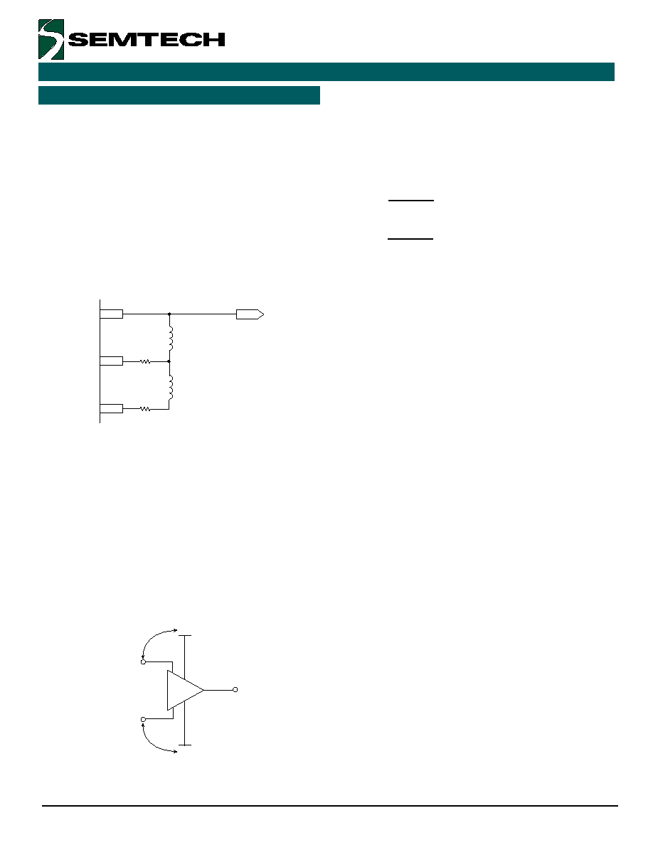
Driver/Comparator/Load Output Circuit
The recommended circuit for combining the driver,
comparator, and load outputs to a single DUT pin is shown
in Figure 1. The inductors in the circuit compensate for
the parasitic capacitance of the load and comparator pins,
minimizing the imaginary part of the impedance to both
incoming and outbound signals. This yields the fastest
driver rise times as well as the smallest amount of
distortion of the signal going into the comparator. The
amount of distortion caused by this compensation network
is small compared to the other sources of distortion.
Figure 22. Optimum Circuit for Combined
Edge720 Outputs
Computing Output Voltage Range
The output voltage range of the driver and load and the
input range of the comparator are a function of VCC
and VEE and their individual voltage overheads, offset,
and gains specified for each.
For example, the driver’s output high range (no load) is
shown below.
Figure 23. Driver Output High Range (no Load)
VINP
DUT Pin
LOAD
DOUT
33
38
40.2
0603
48.7
0805
30
8.2 nh
0603
3.3 nh
0603
Transmission Line
For DOUT(high) of +11.75V, DVH may need to be
overdrived as follows:
+ Offset (of DOUT vs. DVH)
i.e.
+ 125 mV = 12.05V = DVH
Hence, VCC(min) needs to be:
+12.05V + Overhead
i.e.
+12.05 + 3.5V = 15.55V
For the application of DOUTmax = +11.75V, VCC must
be greater than 15.55V. Similar is true for all input/
output ranges specified.
Power Supply Bypassing
Each section of the Edge720 has separate VCC and GND
pins which are not connected to each other internally, so
each ground pin must be connected to analog ground by
the shortest possible path, and each of the VCC pins must
have power and a bypass capacitor provided. These bypass
capacitors should be placed as close to the power pin as
possible for optimum filtering and stability. Pins 31 and
32 provide VCC to the driver circuit.
Pins 21 and 22
connect the driver GND. Pin 4 is VCC, and pin 9 is GND
for the comparator circuit. Pin 49 provides VCC and pins
37 and 46 provide GND to the load circuit.
All of the VEE pins are connected together via the exposed
heat slug on the bottom of the part. Each of these go to
separate sections of the part, so should be bypassed
separately for best noise filtering and stability. Pin 21 and
22 provide VEE to the driver circuit, pin 1 provides it to the
comparator, and pin 52 connects VEE to the load circuit.
+11.75V
0.985
(
)
+11.75V
GAIN
(
DVH
DVL
DOUT
VCC
VEE
Overhead = +3.5V
相关PDF资料 |
PDF描述 |
|---|---|
| E728-EDGE728 | Very High-Speed Dual- and Quad-Channel ECL Delay Lines |
| E737-EDGE737 | Per-Pin Precision Measurement Unit |
| E749-EDGE749 | Octal Pin Electronics Driver / Receiver |
| E818-EDGE818 | Octal 18 V Pin Electronics Driver / Window Comparator |
| E819-EDGE819 | Octal 18 V Pin Electronics Driver |
相关代理商/技术参数 |
参数描述 |
|---|---|
| E72106-000 | 制造商:TE Connectivity 功能描述:DWP-125-1/2-0-80MM - Bulk |
| E72-12V | 制造商:GILWAY 制造商全称:Gilway Technical Lamp 功能描述:Engineering Catalog 169 |
| E722455 | 制造商:Elo Touch Solutions Inc 功能描述:1520 TOUCHCOMPUTER - 15-INCH LCD, ACCUTOUCH (RESISTIVE), USB - Bulk |
| E72246-000 | 功能描述:可复位保险丝 250V .08A-HD 3A MAX (R) RoHS:否 制造商:Bourns 电流额定值: 电阻:7.5 Ohms 最大直流电压: 保持电流:0.1 A 安装风格:SMD/SMT 端接类型:SMD/SMT 跳闸电流:0.6 A 引线间隔: 系列:MF-PSHT 工作温度范围:- 40 C to + 125 C |
| E72382-000 | 制造商:TE Connectivity 功能描述:MTCPQKT2P22SGBD |
发布紧急采购,3分钟左右您将得到回复。