- 您现在的位置:买卖IC网 > PDF目录97873 > E728-EDGE728 Very High-Speed Dual- and Quad-Channel ECL Delay Lines PDF资料下载
参数资料
| 型号: | E728-EDGE728 |
| 英文描述: | Very High-Speed Dual- and Quad-Channel ECL Delay Lines |
| 中文描述: | 极高速双和四通道ECL延迟线 |
| 文件页数: | 14/18页 |
| 文件大小: | 133K |
| 代理商: | E728-EDGE728 |
5
2000 Semtech Corp.
www .semtech.com
HIGH-PERFORMANCE PRODUCTS – ATE
Edge728
Circuit Description (continued)
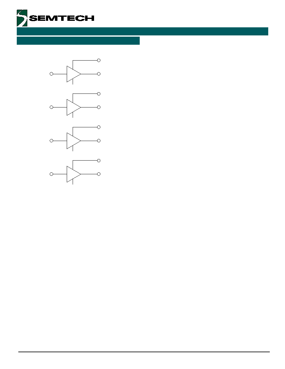
Figure 3. Mode 0 Functional Diagram
Analog Delay Inputs
VDELAY and VWIDTH are high input impedance analog
voltage inputs which control the delay of the rising and
falling edge. VWIDTH can vary from –0.1V to –1.1V, and
VDELAY can vary from –0.2V to –1.1V. When both inputs
are –1.1V, a maximum delay results.
If mode 0 is used, connect all VWIDTH inputs to GND.
Also, connect any unused VDELAY and VWIDTH inputs to
GND.
Mode 2
Mode 2 allows independent adjustment of the rising and
falling edges (see Figures 4 and 5). The propagation delay
for a rising edge is defined as
Tpd+ = Tpd(min) + Tspan
where Tpd(min) is the raw propagation delay of the part
with minimum programmed delay, and Tspan is the
additional delay programmed via the VDELAY input.
The propagation delay for a falling edge is defined as
Tpd–
= Tpd(min) + Tspan + Twidth
where Twidth is defined as the additional delay incurred
by adjusting the VWIDTH input. Notice that Twidth can be
either positive or negative, allowing the part to either
expand or contract an input signal (see Figure 4).
Notice also that Tpd+ is a function of VDELAY only, while
Tpd– is a function of VDELAY and VWIDTH. The transfer
function for Tspan vs. VDELAY is shown for both modes in
Figure 4. The transfer function for Twidth vs. VWIDTH and
VDELAY is shown in Figure 6.
REXT2
REXT2 is an analog current input used to establish the
bias current of the delay cells. An external resistor of
2.74 K
should be connected between REXT2 and ground.
The voltage on REXT2 is forced to ~ –1.34V, producing
an input current of (1.34V) / 2.74 K
= 489 A.
COMP2
COMP2 is an op amp compensation pin and requires an
external capacitor of 0.01
F (X7R type) connected to
either VEE or ground.
OUT1, OUT1*
IN1, IN1*
VDELAY1
T
IN2, IN2*
T
IN3, IN3*
T
IN4, IN4*
T
OUT2, OUT2*
VDELAY2
OUT3, OUT3*
VDELAY3
OUT4, OUT4*
VDELAY4
相关PDF资料 |
PDF描述 |
|---|---|
| E737-EDGE737 | Per-Pin Precision Measurement Unit |
| E749-EDGE749 | Octal Pin Electronics Driver / Receiver |
| E818-EDGE818 | Octal 18 V Pin Electronics Driver / Window Comparator |
| E819-EDGE819 | Octal 18 V Pin Electronics Driver |
| E82802AB | |
相关代理商/技术参数 |
参数描述 |
|---|---|
| E72980-000 | 制造商:TE Connectivity 功能描述:55PC2131-18-2/4/6-9CS2970 - Cable Rools/Shrink Tubing |
| E729PIB-D2192/50 | 制造商:Ferraz Shawmut 功能描述: |
| E72U | 制造商:Thomas & Betts 功能描述:RING TONGUE TERMINAL |
| E73 | 功能描述:灯 Std Glass Wedge 14V .08A .3M RoHS:否 制造商:Chicago Miniature 灯类型:Incandescent 灯座类型:Wire Terminal 灯大小:T-1 3/4 颜色: 电压:14 V 工作电流: MSCP:0.3 MSCP 寿命:40000 hr 封装:Bulk |
发布紧急采购,3分钟左右您将得到回复。