- 您现在的位置:买卖IC网 > PDF目录93349 > EDI88512CA 512Kx8 Monolithic SRAM(512Kx8 CMOS单片静态RAM) PDF资料下载
参数资料
| 型号: | EDI88512CA |
| 英文描述: | 512Kx8 Monolithic SRAM(512Kx8 CMOS单片静态RAM) |
| 中文描述: | 512Kx8单片的SRAM(512Kx8的CMOS单片静态内存) |
| 文件页数: | 1/9页 |
| 文件大小: | 181K |
| 代理商: | EDI88512CA |
1
White Electronic Designs Corporation (602) 437-1520 www.whiteedc.com
HI-RELIABILITY PRODUCT
EDI88512CA
512Kx8 Monolithic SRAM, SMD 5962-95600
FEATURES
s Access Times of 15, 17, 20, 25, 35, 45, 55ns
s Data Retention Function (LPA version)
s TTL Compatible Inputs and Outputs
s Fully Static, No Clocks
s Organized as 512Kx8
s Commercial, Industrial and Military Temperature Ranges
s 32 lead JEDEC Approved Evolutionary Pinout
Ceramic Sidebrazed 600 mil DIP (Package 9)
Ceramic Sidebrazed 400 mil DIP (Package 326)
Ceramic 32 pin Flatpack (Package 344)
Ceramic Thin Flatpack (Package 321)
Ceramic SOJ (Package 140)
s 36 lead JEDEC Approved Revolutionary Pinout
Ceramic Flatpack (Package 316)
Ceramic SOJ (Package 327)
Ceramic LCC (Package 502)
s Single +5V (
±10%) Supply Operation
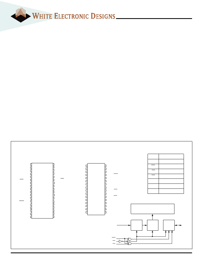
36 PIN
TOP VIEW
August 1999 Rev. 8
PIN DESCRIPTION
I/O0-7
Data Inputs/Outputs
A0-18
Address Inputs
WE
Write Enables
CS
Chip Selects
OE
Output Enable
VCC
Power (+5V
±10%)
VSS
Ground
NC
Not Connected
BLOCK DIAGRAM
Memory Array
Address
Buffer
Address
Decoder
I/O
Circuits
A-18
I/O-7
WE
CS
OE
FIG. 1
PIN CONFIGURATION
The EDI88512CA is a 4 megabit Monolithic CMOS Static RAM.
The 32 pin DIP pinout adheres to the JEDEC evolutionary standard
for the four megabit device. All 32 pin packages are pin for pin
upgrades for the single chip enable 128K x 8, the EDI88128CS.
Pins 1 and 30 become the higher order addresses.
The 36 pin revolutionary pinout also adheres to the JEDEC stan-
dard for the four megabit device. The center pin power and ground
pins help to reduce noise in high performance systems. The 36 pin
pinout also allows the user an upgrade path to the future 2Mx8.
A Low Power version with Data Retention (EDI88512LPA) is also
available for battery backed applications. Military product is
available compliant to Appendix A of MIL-PRF-38535.
32 PIN
TOP VIEW
1
2
3
4
5
6
7
8
9
10
11
12
13
14
15
16
17
18
36
35
34
33
32
31
30
29
28
27
26
25
24
23
22
21
20
19
A0
A1
A2
A3
A4
CS
I/O0
I/O1
Vcc
Vss
I/O2
I/O3
WE
A5
A6
A7
A8
A9
NC
A18
A17
A16
A15
OE
I/O7
I/O6
VSS
VCC
I/O5
I/O4
A14
A13
A12
A11
A10
NC
36 pin
Revolutionary
32
31
30
29
28
27
26
25
24
23
22
21
20
19
18
17
1
2
3
4
5
6
7
8
9
10
11
12
13
14
15
16
VCC
A15
A17
WE
A13
A8
A9
A11
OE
A10
CS
I/O7
I/O6
I/O5
I/O4
I/O3
A18
A16
A14
A12
A7
A6
A5
A4
A3
A2
A1
A
I/O
I/O1
I/O2
VSS
Evolutionary
32 pin
相关PDF资料 |
PDF描述 |
|---|---|
| EDI88512C | 512Kx8 Monolithic SRAM(512Kx8 CMOS单片静态RAM) |
| EDI8C32128C | 128Kx32 SRAM Module(低功耗CMOS,512Kx32静态RAM模块(存取时间15,17,20,25,35,45,55ns)) |
| EDI8C32512CA | 512Kx32 SRAM Module(低功耗CMOS,128Kx32静态RAM模块(存取时间15,17,20,25,35,45,55ns)) |
| EDI8C32512LPA20EC | Integrated Buffers with VCOM; Temperature Range: -40°C to 85°C; Package: 20-HTSSOP T&R |
| EDI8C32512LPA20EI | Integrated Buffers with VCOM; Temperature Range: -40°C to 85°C; Package: 24-HTSSOP |
相关代理商/技术参数 |
参数描述 |
|---|---|
| EDI88512CA/LPA-B32 | 制造商:未知厂家 制造商全称:未知厂家 功能描述:SRAM |
| EDI88512CA/LPA-C | 制造商:未知厂家 制造商全称:未知厂家 功能描述:SRAM |
| EDI88512CA/LPA-F32 | 制造商:未知厂家 制造商全称:未知厂家 功能描述:SRAM |
| EDI88512CA/LPA-F36 | 制造商:未知厂家 制造商全称:未知厂家 功能描述:SRAM |
| EDI88512CA/LPA-K | 制造商:未知厂家 制造商全称:未知厂家 功能描述:SRAM |
发布紧急采购,3分钟左右您将得到回复。