- 您现在的位置:买卖IC网 > PDF目录97893 > EDL1216AASA-75 Programmable VCOM; Temperature Range: -40°C to 85°C; Package: 12-DFN T&R PDF资料下载
参数资料
| 型号: | EDL1216AASA-75 |
| 英文描述: | Programmable VCOM; Temperature Range: -40°C to 85°C; Package: 12-DFN T&R |
| 中文描述: | 内存| 4X2MX16 |的CMOS | BGA封装| 54PIN |塑料 |
| 文件页数: | 1/59页 |
| 文件大小: | 489K |
| 代理商: | EDL1216AASA-75 |
当前第1页第2页第3页第4页第5页第6页第7页第8页第9页第10页第11页第12页第13页第14页第15页第16页第17页第18页第19页第20页第21页第22页第23页第24页第25页第26页第27页第28页第29页第30页第31页第32页第33页第34页第35页第36页第37页第38页第39页第40页第41页第42页第43页第44页第45页第46页第47页第48页第49页第50页第51页第52页第53页第54页第55页第56页第57页第58页第59页
Document No. E0196E20 (Ver. 2.0)
Date Published March 2002 (K) Japan
URL: http://www.elpida.com
Elpida Memory, Inc. 2001-2002
DATA SHEET
128M bits Mobile RAM
EDL1216AASA (8M words
×××× 16 bits)
Description
The EDL1216AA is a 128M bits Mobile RAM organized
as 2,097,152 words
× 16 bits × 4 banks. The low
power synchronous DRAMs achieved low power
consumption and high-speed data transfer using the
pipeline architecture.
All inputs and outputs are
synchronized with the positive edge of the clock.
This product is packaged in 54-ball FBGA.
Features
Low power supply
VDD:
2.5V
± 0.2V
VDDQ: 1.8V ± 0.15V
Wide temperature range (25°C to 85°C)
Programmable partial self refresh
Programmable driver strength
Programmable temperature compensated self refresh
(Option)
Deep power down mode
Small package (54-ball FBGA)
Fully Synchronous Dynamic RAM, with all signals
referenced to a positive clock edge
Pulsed interface
Possible to assert random column address in every
cycle
Quad internal banks controlled by BA0 (A13) and
BA1 (A12)
Byte control by LDQM and UDQM
Wrap sequence = Sequential / Interleave
/CAS latency (CL) = 2, 3
Automatic precharge and controlled precharge
Auto refresh and self refresh
×16 organization
4,096 refresh cycles/64ms
Burst termination by Burst stop command and
Precharge command
Applications
Mobile cellular handset, PDA, wireless PDA, handheld
PC, home electronic appliances, and information
appliances, etc.
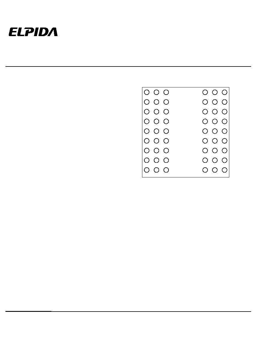
Pin Configurations
/xxx indicates active low signal.
VSS
1
A
B
C
D
E
F
G
H
J
23456789
DQ14
DQ12
DQ10
DQ8
UDQM
NC
A8
VSS
DQ15
DQ13
DQ11
DQ9
NC
CLK
A11
A7
A5
VSSQ
VDDQ
VSSQ
VDDQ
VSS
CKE
A9
A6
A4
VDDQ
VSSQ
VDDQ
VSSQ
VDD
/CAS
BA0
A0
A3
DQ0
DQ2
DQ4
DQ6
LDQM
/RAS
BA1
A1
A2
VDD
DQ1
DQ3
DQ5
DQ7
/WE
/CS
A10
VDD
(Top view)
A0 to A11
Address inputs
BA0, BA1
Bank Select
DQ0 to DQ15
Data inputs / outputs
CLK
Clock input
CKE
Clock enable
/CS
Chip select
/RAS
Row address strobe
/CAS
Column address strobe
/WE
Write enable
UDQM
Upper DQ mask enable
LDQM
Lower DQ mask enable
VDD
Supply voltage
VSS
Ground
VDDQ
Supply voltage for DQ
VSSQ
Ground for DQ
NC
No connect
相关PDF资料 |
PDF描述 |
|---|---|
| EDL1216BASA-75 | Programmable VCOM; Temperature Range: -40°C to 85°C; Package: 12-DFN T&R |
| EDL1216CASA-10 | Programmable VCOM; Temperature Range: -40°C to 85°C; Package: 24-QFN |
| EDS1232AABB-60 | Programmable VCOM; Temperature Range: -40°C to 85°C; Package: 24-QFN |
| EDS1232AABB-60L | Programmable VCOM; Temperature Range: -40°C to 85°C; Package: 24-QFN T&R |
| EDS1232AABB-75 | Programmable VCOM; Temperature Range: -40°C to 85°C; Package: 24-QFN T&R |
相关代理商/技术参数 |
参数描述 |
|---|---|
| EDL1216AASA-75-E | 制造商:ELPIDA 制造商全称:Elpida Memory 功能描述:128M bits Mobile RAM |
| EDL1216BASA-75 | 制造商:未知厂家 制造商全称:未知厂家 功能描述:SDRAM|4X2MX16|CMOS|BGA|54PIN|PLASTIC |
| EDL1216CASA | 制造商:ELPIDA 制造商全称:Elpida Memory 功能描述:128M bits Mobile RAM |
| EDL1216CASA-10 | 制造商:未知厂家 制造商全称:未知厂家 功能描述:SDRAM|4X2MX16|CMOS|BGA|54PIN|PLASTIC |
| EDL1216CASA-10-E | 制造商:ELPIDA 制造商全称:Elpida Memory 功能描述:128M bits Mobile RAM |
发布紧急采购,3分钟左右您将得到回复。