- 您现在的位置:买卖IC网 > Datasheet目录411 > EK64904-01 (Peregrine Semiconductor)KIT EVAL FOR 64904 NO CABLES Datasheet资料下载
参数资料
| 型号: | EK64904-01 |
| 厂商: | Peregrine Semiconductor |
| 文件页数: | 3/11页 |
| 文件大小: | 0K |
| 描述: | KIT EVAL FOR 64904 NO CABLES |
| 标准包装: | 1 |
| 系列: | UltraCMOS™ |
| 类型: | 数字调谐式电容器 |
| 频率: | 100MHz ~ 3GHz |
| 适用于相关产品: | PE64904 |
| 已供物品: | 板 |
| 其它名称: | EK64904-1 EK64904-1-ND |
�� �
�
�PE64904�
�Product� Specification�
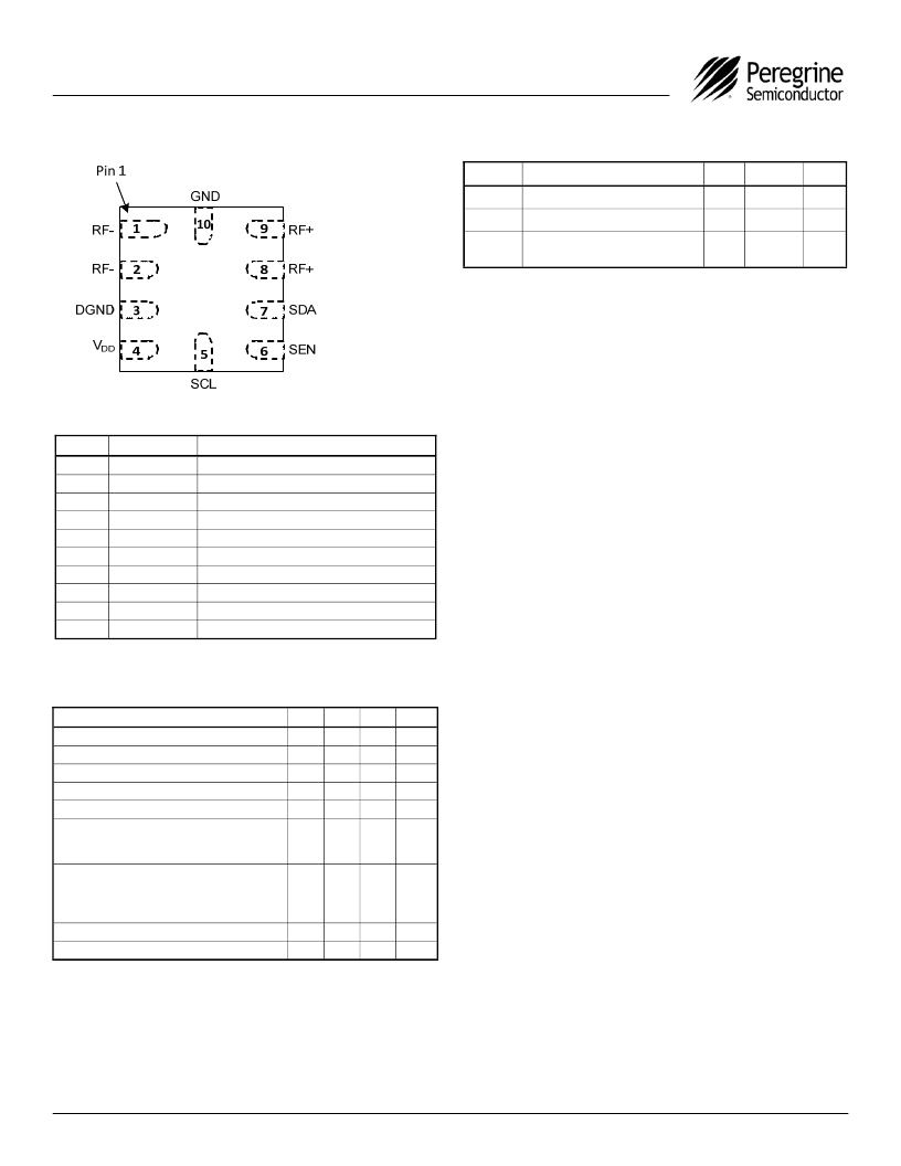
�Figure� 3.� Pin� Configuration� (Top� View)�
�Table� 4.� Absolute� Maximum� Ratings�
�Symbol�
�V� DD�
�V� I�
�V� ESD�
�Parameter/Conditions�
�Power� supply� voltage�
�Voltage� on� any� DC� input�
�ESD� Voltage� (HBM,� MIL_STD�
�883� Method� 3015.7)�
�Min�
�-0.3�
�-0.3�
�Max�
�4.0�
�4.0�
�1500�
�Units�
�V�
�V�
�V�
�Exceeding� absolute� maximum� ratings� may� cause�
�permanent� damage.� Operation� should� be� restricted�
�to� the� limits� in� the� Operating� Ranges� table.�
�Operation� between� operating� range� maximum� and�
�absolute� maximum� for� extended� periods� may� reduce�
�reliability.�
�Table� 2.� Pin� Descriptions�
�Electrostatic� Discharge� (ESD)� Precautions�
�Negative� RF� Port�
�Pin� #�
�1�
�2�
�3�
�4�
�5�
�6�
�7�
�8�
�9�
�10�
�Pin� Name�
�RF-�
�RF-�
�DGND�
�V� DD�
�SCL�
�SEN�
�SDA�
�RF+�
�RF+�
�GND�
�Description�
�1�
�Negative� RF� Port� 1�
�Ground�
�Power� supply� pin�
�Serial� interface� Clock� input�
�Serial� Interface� Latch� Enable� Input�
�Serial� interface� Data� input�
�Positive� RF� Port� 1�
�Positive� RF� Port� 1�
�RF� Ground�
�When� handling� this� UltraCMOS� ?� device,� observe�
�the� same� precautions� that� you� would� use� with� other�
�ESD-sensitive� devices.� Although� this� device�
�contains� circuitry� to� protect� it� from� damage� due� to�
�ESD,� precautions� should� be� taken� to� avoid�
�exceeding� the� specified� rating.� ?�
�?�
�Latch-Up� Avoidance�
�Unlike� conventional� CMOS� devices,� UltraCMOS� ?�
�devices� are� immune� to� latch-up.�
�Note� 1:� Pins� 1-2� and� 8-9� must� be� tied� together� on� PCB� for� optimal� performance.�
�Moisture� Sensitivity� Level�
�Table� 3.� Operating� Ranges�
�The� Moisture� Sensitivity� Level� rating� for� the�
�Parameter�
�V� DD� Supply� Voltage�
�I� DD� Power� Supply� Current� (V� DD� =� 2.6V)�
�Min�
�2.3�
�Typ�
�2.6�
�140�
�Max�
�3.6�
�200�
�Units�
�V�
�μA�
�PE64904� in� the� 10-lead� 2� x� 2� x� 0.45� mm� QFN�
�package� is� MSL1.�
�I� DD� Standby� Current� (V� DD� =� 2.6V)�
�25�
�μA�
�V� IH� Control� Voltage� High�
�V� IL� Control� Voltage� Low�
�1.2�
�0�
�1.8�
�0�
�3.6�
�0.57�
�V�
�V�
�RF� Input� Power� (50� ?� )� 1�
�698� -� 915� MHz�
�1710� -1910� MHz�
�Peak� Operating� RF� Voltage� 2�
�V� P� to� V� M�
�V� P� to� RFGND�
�V� M� to� RFGND�
�+34�
�+32�
�30�
�30�
�30�
�dBm�
�dBm�
�Vpk�
�Vpk�
�Vpk�
�T� OP� Operating� Temperature� Range�
�T� ST� Storage� Temperature� Range�
�-40�
�-65�
�+85�
�+150�
�°C�
�°C�
�Notes:� 1.� Maximum� Power� Available� from� 50� ?� Source.� Pulsed� RF� input� with�
�4620� μS� period,� 50%� duty� cycle,� measured� per� 3GPP� TS� 45.005.�
�2.� Node� voltages� defined� per� Equivalent� Circuit� Model� Schematic�
�(� Figure� 18� ).� When� DTC� is� used� as� a� part� of� reactive� network,� impedance�
�transformation� may� cause� the� internal� RF� voltages� (V� P� ,� V� M� )� to� exceed� Peak�
�Operating� RF� Voltage� even� with� specified� RF� Input� Power� Levels.� For�
�operation� above� about� +20� dBm� (100� mW),� the� complete� RF� circuit� must�
�be� simulated� using� actual� input� power� and� load� conditions,� and� internal�
�node� voltages� (V� P� ,� V� M� in� Figure� 18� )� monitored� to� not� exceed� 30� Vpk.�
�Document� No.� 70-0325-06� │� www.psemi.com�
�?2011-2012� Peregrine� Semiconductor� Corp.� All� rights� reserved.�
�Page� 3� of� 11�
�Logo� updated� under� non-rev� change.� Peregrine� products� are� protected� under� one� or� more� of� the� following� U.S.� Patents:� http://patents.psemi.com�
�相关PDF资料 |
PDF描述 |
|---|---|
| EK64905-11 | KIT EVAL FOR 64904 W/CABLES |
| EKL3104 | D-IMAGER 3D IMAGE SENSOR |
| EKL3105 | 3D IMAGE SENSOR-HIGH PRECISION |
| EKL3106 | 3D IMAGE SENSOR-HIGH PRECISION |
| EKMB1301111K | SENSOR PIR |
相关代理商/技术参数 |
参数描述 |
|---|---|
| EK64904-11 | 功能描述:KIT EVAL FOR 64904 W/CABLES RoHS:是 类别:RF/IF 和 RFID >> RF 评估和开发套件,板 系列:UltraCMOS™ 标准包装:1 系列:- 类型:GPS 接收器 频率:1575MHz 适用于相关产品:- 已供物品:模块 其它名称:SER3796 |
| EK64904-12 | 制造商:Peregrine Semiconductor 功能描述:RF EVAL FOR PE64904 制造商:Peregrine Semiconductor 功能描述:DIGITALLY TUNABLE CAPACITOR EVALUATION BOARD 制造商:Peregrine Semiconductor 功能描述:EVALUATION KIT FOR PE64904 |
| EK64905-01 | 功能描述:KIT EVAL FOR 64904 NO CABLES RoHS:是 类别:RF/IF 和 RFID >> RF 评估和开发套件,板 系列:UltraCMOS™ 标准包装:1 系列:- 类型:GPS 接收器 频率:1575MHz 适用于相关产品:- 已供物品:模块 其它名称:SER3796 |
| EK64905-11 | 功能描述:KIT EVAL FOR 64904 W/CABLES RoHS:是 类别:RF/IF 和 RFID >> RF 评估和开发套件,板 系列:UltraCMOS™ 标准包装:1 系列:- 类型:GPS 接收器 频率:1575MHz 适用于相关产品:- 已供物品:模块 其它名称:SER3796 |
| EK64905-12 | 制造商:Peregrine Semiconductor 功能描述:RF EVAL FOR PE64905 制造商:Peregrine Semiconductor 功能描述:DIGITALLY TUNABLE CAPACITOR EVALUATION BOARD |
发布紧急采购,3分钟左右您将得到回复。