参数资料
| 型号: | EL2142CSZ-T7 |
| 厂商: | Intersil |
| 文件页数: | 4/6页 |
| 文件大小: | 0K |
| 描述: | IC LINE RECEIVER DIFF IN 8-SOIC |
| 标准包装: | 1 |
| 放大器类型: | 差分 |
| 电路数: | 1 |
| 转换速率: | 400 V/µs |
| 增益带宽积: | 200MHz |
| -3db带宽: | 150MHz |
| 电流 - 输入偏压: | 6µA |
| 电压 - 输入偏移: | 10000µV |
| 电流 - 电源: | 11mA |
| 电流 - 输出 / 通道: | 60mA |
| 电压 - 电源,单路/双路(±): | 6 V ~ 12.6 V,±3 V ~ 6.3 V |
| 工作温度: | -40°C ~ 85°C |
| 安装类型: | 表面贴装 |
| 封装/外壳: | 8-SOIC(0.154",3.90mm 宽) |
| 供应商设备封装: | 8-SOIC |
| 包装: | 标准包装 |
| 其它名称: | EL2142CSZ-T7DKR |
4
FN7049.1
February 11, 2005
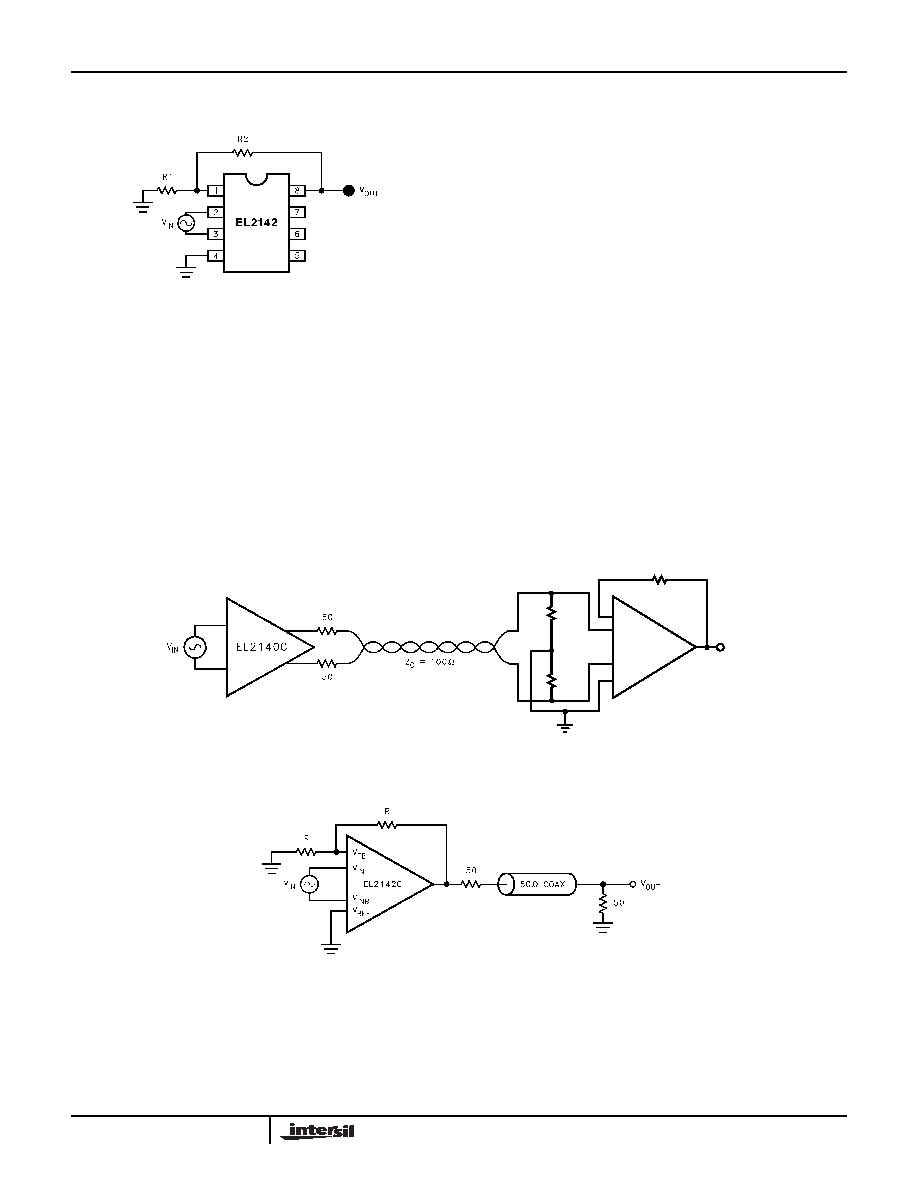
Applications Information
Gain Equation
VOUT = ((R2+R1)/R1) x (VIN-VINB+VREF) when R1 tied to
GND
VOUT = ((R2+R1)/R1) x (VIN-VINB) when R1 tied to VREF
Choice of Feedback Resistor
For a gain of one, VOUT may be shorted back to VFB, but
100
Ω-200Ω improves the bandwidth. For gains greater than
one, there is little to be gained from choosing resistor R1
value below 200
Ω, for it would only result in increased power
dissipation and potential signal distortion. Above 200
Ω, the
bandwidth response will develop some peaking (for a gain of
one), but substantially higher R1 values may be used for
higher voltage gains, such as up to 1k
Ω at a gain of four
before peaking will develop.
Capacitance Considerations
As with many high bandwidth amplifiers, the EL2142 prefers
not to drive highly capacitive loads. It is best if the
capacitance on VOUT is kept below 10pF if the user does not
want gain peaking to develop. The VFB node forms a
potential pole in the feedback loop, so capacitance should
be minimized on this node for maximum bandwidth.
The amount of capacitance tolerated on any of these nodes
in an actual application will also be dependent on the gain
setting and the resistor values in the feedback network.
Typical Applications Circuits
FIGURE 1. TYPICAL TWISTED PAIR APPLICATION
50
Ω
VFB
50
Ω
EL2142
VIN
VINB
VREF
VOUT
100
Ω
FIGURE 2. COAXIAL CABLE DRIVER PAIR APPLICATION
EL2142
相关PDF资料 |
PDF描述 |
|---|---|
| 3403.0123.24 | FUSE 5A 125VAC SMD SLOW |
| SSW-150-01-S-S | CONN RCPT .100" 50POS SNGL GOLD |
| 0741620012 | CONN RCPT R/A 12POS 2.54MM TIN |
| 3403.0120.24 | FUSE 2.5A 125VAC SMD SLOW |
| EL2141CSZ-T7 | IC DRVR TWISTED PR 150MHZ 8-SOIC |
相关代理商/技术参数 |
参数描述 |
|---|---|
| EL215 | 功能描述:晶体管输出光电耦合器 Optocouplers RoHS:否 制造商:Vishay Semiconductors 输入类型:DC 最大集电极/发射极电压:70 V 最大集电极/发射极饱和电压:0.4 V 绝缘电压:5300 Vrms 电流传递比:100 % to 200 % 最大正向二极管电压:1.65 V 最大输入二极管电流:60 mA 最大集电极电流:100 mA 最大功率耗散:100 mW 最大工作温度:+ 110 C 最小工作温度:- 55 C 封装 / 箱体:DIP-4 封装:Bulk |
| EL215(TA) | 功能描述:晶体管输出光电耦合器 Optocouplers RoHS:否 制造商:Vishay Semiconductors 输入类型:DC 最大集电极/发射极电压:70 V 最大集电极/发射极饱和电压:0.4 V 绝缘电压:5300 Vrms 电流传递比:100 % to 200 % 最大正向二极管电压:1.65 V 最大输入二极管电流:60 mA 最大集电极电流:100 mA 最大功率耗散:100 mW 最大工作温度:+ 110 C 最小工作温度:- 55 C 封装 / 箱体:DIP-4 封装:Bulk |
| EL215(TA)-V | 功能描述:晶体管输出光电耦合器 Optocouplers RoHS:否 制造商:Vishay Semiconductors 输入类型:DC 最大集电极/发射极电压:70 V 最大集电极/发射极饱和电压:0.4 V 绝缘电压:5300 Vrms 电流传递比:100 % to 200 % 最大正向二极管电压:1.65 V 最大输入二极管电流:60 mA 最大集电极电流:100 mA 最大功率耗散:100 mW 最大工作温度:+ 110 C 最小工作温度:- 55 C 封装 / 箱体:DIP-4 封装:Bulk |
| EL215(TB) | 功能描述:晶体管输出光电耦合器 Optocouplers RoHS:否 制造商:Vishay Semiconductors 输入类型:DC 最大集电极/发射极电压:70 V 最大集电极/发射极饱和电压:0.4 V 绝缘电压:5300 Vrms 电流传递比:100 % to 200 % 最大正向二极管电压:1.65 V 最大输入二极管电流:60 mA 最大集电极电流:100 mA 最大功率耗散:100 mW 最大工作温度:+ 110 C 最小工作温度:- 55 C 封装 / 箱体:DIP-4 封装:Bulk |
| EL215(TB)-V | 功能描述:晶体管输出光电耦合器 Optocouplers RoHS:否 制造商:Vishay Semiconductors 输入类型:DC 最大集电极/发射极电压:70 V 最大集电极/发射极饱和电压:0.4 V 绝缘电压:5300 Vrms 电流传递比:100 % to 200 % 最大正向二极管电压:1.65 V 最大输入二极管电流:60 mA 最大集电极电流:100 mA 最大功率耗散:100 mW 最大工作温度:+ 110 C 最小工作温度:- 55 C 封装 / 箱体:DIP-4 封装:Bulk |
发布紧急采购,3分钟左右您将得到回复。