参数资料
| 型号: | EL4501IUZ |
| 厂商: | Intersil |
| 文件页数: | 8/19页 |
| 文件大小: | 0K |
| 描述: | IC VIDEO FRONT END AMP 24-QSOP |
| 标准包装: | 55 |
| 应用: | 视频前端(VFE) |
| 电路数: | 1 |
| -3db带宽: | 100MHz |
| 转换速率: | 96 V/µs |
| 电流 - 电源: | 10.5mA |
| 电流 - 输出 / 通道: | 70mA |
| 电压 - 电源,单路/双路(±): | 4.5 V ~ 5.5 V |
| 安装类型: | 表面贴装 |
| 封装/外壳: | 24-SSOP(0.154",3.90mm 宽) |
| 供应商设备封装: | 24-QSOP |
| 包装: | 管件 |
| 产品目录页面: | 1233 (CN2011-ZH PDF) |
16
prevents the amplifier output drifting significantly from the
DC-restore reference level. This improves start-up behavior
and speeds recovery after a signal drop-out. For ease of
use, the EL4501 provides a buffered 1.3V DC level normally
connected directly to the restore loop reference input (REF
IN). Alternatively, an external voltage between 0V and 3.5V,
connected to REF IN, can be used to set the restored level.
Auto-Zero Loop Bandwidth
The gain bandwidth product (GBWP) of the auto-zero loop is
determined by the size of the hold capacitor and the
transconductance (gM1) of the sample and hold amplifier.
GBWP = gM1/(2π * CH), gM1 is about 1/(29kΩ), for
CH = 270pF, GBWP is 20kHz. For CH = 100pF, GBWP is
about 55kHz.
Charge Injection and Hold Step Error
Charge injection refers to the charge transferred to the hold
capacitor when switching to the hold mode. The charge
should ideally be 0, but due to stray capacitive coupling and
other effects, it is typically 6fC. This charge changes the hold
capacitor voltage by
ΔV = ΔQ/CH and will shift the output
voltage of the video amplifier by
ΔV. However, this shift is
small and can be negligible for the EL4501 (see the Hold
Step Voltage Error vs Hold Capacitance curve). Assuming
CH = 100pF, ΔV is about 60V. There will be 60V change at
the video amplifier output.
Droop Rate
When the S/H amplifier is in the hold mode, there is a small
current that leaks from the switch to the hold capacitor. This
quantity is called the droop current. This droop current
produces a ramp in the hold capacitor voltage, which in turn
produces a similar voltage at the video amplifier output. The
droop rate at the video amplifier output can be found using
the following equation:
Assuming CH = 100pF, from the Droop Rate vs Hold
Capacitance curve, the droop rate is about 0.31mV/ms at the
video amplifier output at room temperature. In NTSC
applications, there is about 60s between auto-zero periods.
Thus, there is (0.31mV/ms) * 60s = 18.6V. It is much less
than 0.5IRE (3.5mV). This drift is negligible.
Choice of Hold Capacitor
The EL4501 allows the user to choose the hold capacitor as
low as 1pF and it is still stable. A smaller hold capacitor has
a faster acquisition time and faster auto-zero loop response,
but would increase the droop and hold step error. Also, if the
acquisition time is too fast, it would probably give an image
with clamp streaking and low frequency noise with noisy
signals. Increasing the hold capacitor would increase the
acquisition time, lower the auto-zero loop response, lower
the droop and hold step error. See the performance curves
for the trade-off. Normally, in video (NTSC and PAL)
applications, a smooth acquisition might takes about 10 to
20 scan lines. For a hold capacitor equal to 270pF, the
acquisition time is about 10 lines. In the worse case, ambient
temperature is 85°C, the droop current is 2.2nA which
causes the output voltage ramp to about 0.49mV for 60s.
This drift is negligible in most applications. Figure 38 shows
the input and output waveforms of the video amplifier while
the S/H is in sample mode. Applying a 1V step to the video
amplifier input, the output of the video amplifier jumps to
2.3V. Then, the auto-zero system tries to drive the video
output to the reference voltage, which is 1.3V. The
acquisition time takes about 10 NTSC scan lines.
-
+
-
+
S/H
VREF_IN
VOUT
VIN
0.1F
gM
~1.8V
CH
GBWP
gM
2
πC
H
---------------
=
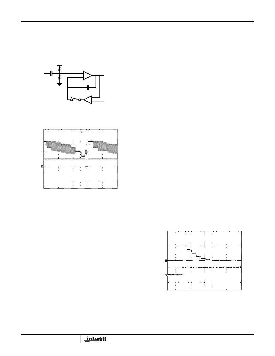
FIGURE 36. DC-RESTORE AMPLIFIER AND S/H
CONFIGURATION
INPUT
VIDEO
SIGNAL
BACK
PORCH
OUTPUT
CH1=500mV/DIV
CH3=5V/DIV
M=10s
FIGURE 37. NTSC VIDEO SIGNAL WITH BACK PORCH
OUTPUT
DroopRate
ΔV
RAMP
Δt
------------------------
=
VIDEO
AMP
OUTPUT
VIDEO
AMP
INPUT
CH=270pF
Auto-zero mechanism restores amplifier output to
1.3V after +1V step at input
CH1=500mV/DIV
CH2=1V/DIV
M=100s
FIGURE 38. INPUT AND OUTPUT WAVEFORMS WITH S/H IN
SAMPLE MODE
EL4501
相关PDF资料 |
PDF描述 |
|---|---|
| LTC1596ACSW | IC D/A CONV 16BIT MLTPLYNG16SOIC |
| DAC8408GPZ | IC DAC 8BIT QUAD W/MEMORY 28DIP |
| AD5542LR | IC DAC 16BIT SERIAL-IN 14-SOIC |
| AD5541LR | IC DAC 16BIT SERIAL-IN 8-SOIC |
| LTC1596ACSW#TRPBF | IC D/A CONV 16BIT MLTPLYNG16SOIC |
相关代理商/技术参数 |
参数描述 |
|---|---|
| EL4501IUZT13 | 制造商:INTERSIL 制造商全称:Intersil Corporation 功能描述:Video Front End |
| EL4501IUZ-T13 | 功能描述:视频 IC EL4501IUZ VID FRONT END RoHS:否 制造商:Fairchild Semiconductor 工作电源电压:5 V 电源电流:80 mA 最大工作温度:+ 85 C 封装 / 箱体:TSSOP-28 封装:Reel |
| EL4501IUZ-T7 | 功能描述:视频 IC EL4501IUZ VID FRONT END RoHS:否 制造商:Fairchild Semiconductor 工作电源电压:5 V 电源电流:80 mA 最大工作温度:+ 85 C 封装 / 箱体:TSSOP-28 封装:Reel |
| EL4501IUZ-T7A | 功能描述:视频 IC EL4501IUZ VID FRONT END RoHS:否 制造商:Fairchild Semiconductor 工作电源电压:5 V 电源电流:80 mA 最大工作温度:+ 85 C 封装 / 箱体:TSSOP-28 封装:Reel |
| EL4502 | 功能描述:高速光耦合器 Optocouplers RoHS:否 制造商:Avago Technologies 电流传递比: 最大波特率: 最大正向二极管电压:1.75 V 最大反向二极管电压:5 V 最大功率耗散:40 mW 最大工作温度:+125 C 最小工作温度:- 40 C 封装 / 箱体:SOIC-5 封装:Tube |
发布紧急采购,3分钟左右您将得到回复。