- 您现在的位置:买卖IC网 > PDF目录97906 > EL5420CR-T7 12MHz Rail-to-Rail Input-Output Op Amps PDF资料下载
参数资料
| 型号: | EL5420CR-T7 |
| 英文描述: | 12MHz Rail-to-Rail Input-Output Op Amps |
| 中文描述: | 12MHz的轨到轨输入输出运算放大器 |
| 文件页数: | 3/13页 |
| 文件大小: | 275K |
| 代理商: | EL5420CR-T7 |
11
EL5220C, EL5420C
12MHz Rail-to-Rail Input-Output Op Amps
E
L
52
20
C
,E
L
54
20
C
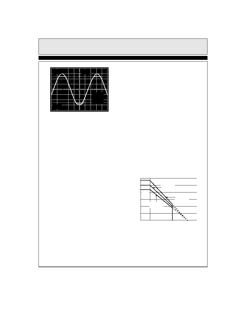
Figure 2. Operation with Beyond-the-Rails
Input
Power Dissipation
With the high-output drive capability of the EL5220C
and EL5420C amplifiers, it is possible to exceed the
125°C “absolute-maximum junction temperature” under
certain load current conditions. Therefore, it is important
to calculate the maximum junction temperature for the
application to determine if load conditions need to be
modified for the amplifier to remain in the safe operating
area.
The maximum power dissipation allowed in a package is
determined according to:
where:
TJMAX = Maximum Junction Temperature
TAMAX= Maximum Ambient Temperature
θJA = Thermal Resistance of the Package
PDMAX = Maximum Power Dissipation in the Package
The maximum power dissipation actually produced by
an IC is the total quiescent supply current times the total
power supply voltage, plus the power in the IC due to the
loads, or:
when sourcing, and:
when sinking.
where
i = 1 to 2 for Dual and 1 to 4 for Quad
VS = Total Supply Voltage
ISMAX = Maximum Supply Current Per Amplifier
VOUTi = Maximum Output Voltage of the Application
ILOADi = Load Current
If we set the two PDMAX equations equal to each other,
we can solve for RLOADi to avoid device overheat. Fig-
ures 3, 4, and 5 provide a convenient way to see if the
device will overheat. The maximum safe power dissipa-
tion can be found graphically, based on the package type
and the ambient temperature. By using the previous
equation, it is a simple matter to see if PDMAX exceeds
the device's power derating curves. To ensure proper
operation, it is important to observe the recommended
derating curves in Figures 3, 4, and 5.
Figure 3. Package Power Dissipation vs
Ambient Temperature
VS=±2.5V
TA=25°C
AV=1
VIN=6VP-P
1V
100s
1V
PDMAX
TJMAX TAMAX
–
ΘJA
------------------------------------------------
=
PDMAX
ΣiVS ISMAX VS+
(
VOUTi) ILOADi
×
–
+
×
[]
×
=
PDMAX
ΣiVS ISMAX VOUTi
(
VS- ) ILOADi
×
–
+
×
[]
×
=
400
800
Po
w
er
Di
ss
ip
at
io
n
(m
W
)
Ambient Temperature (°C)
0
1200
MAX TJ=125°C
1000
600
200
TSSOP14
θJA=100°C/W
25
50
75
100
125
150
85
JEDEC JESD51-7 High Effective Thermal Conductivity (4-
Layer) Test Board
LPP exposed diepad soldered to PCB per JESD51-5
1.136W
SO14
θJA=88°C/W
1.0W
870mW
MSOP8
θJA=115°C/W
相关PDF资料 |
PDF描述 |
|---|---|
| EL5420CL | 12MHz Rail-to-Rail Input-Output Op Amps |
| EL5420CL-T7 | 12MHz Rail-to-Rail Input-Output Op Amps |
| EL5420CR | 12MHz Rail-to-Rail Input-Output Op Amps |
| EL5420CS | 12MHz Rail-to-Rail Input-Output Op Amps |
| EL5420CS-T13 | 12MHz Rail-to-Rail Input-Output Op Amps |
相关代理商/技术参数 |
参数描述 |
|---|---|
| EL5420CRZ | 功能描述:高速运算放大器 EL5420CRZ 12MHZ QUAD RAIL INPUTOUTPUT OP RoHS:否 制造商:Texas Instruments 通道数量:1 电压增益 dB:116 dB 输入补偿电压:0.5 mV 转换速度:55 V/us 工作电源电压:36 V 电源电流:7.5 mA 最大工作温度:+ 85 C 安装风格:SMD/SMT 封装 / 箱体:SOIC-8 封装:Tube |
| EL5420CRZ-T13 | 功能描述:高速运算放大器 EL5420CRZ 12 MHZ QD R2R I/O OP RoHS:否 制造商:Texas Instruments 通道数量:1 电压增益 dB:116 dB 输入补偿电压:0.5 mV 转换速度:55 V/us 工作电源电压:36 V 电源电流:7.5 mA 最大工作温度:+ 85 C 安装风格:SMD/SMT 封装 / 箱体:SOIC-8 封装:Tube |
| EL5420CRZ-T7 | 功能描述:高速运算放大器 EL5420CRZ 12 MHZ QD R2R I/O OP RoHS:否 制造商:Texas Instruments 通道数量:1 电压增益 dB:116 dB 输入补偿电压:0.5 mV 转换速度:55 V/us 工作电源电压:36 V 电源电流:7.5 mA 最大工作温度:+ 85 C 安装风格:SMD/SMT 封装 / 箱体:SOIC-8 封装:Tube |
| EL5420CRZ-T7A | 功能描述:运算放大器 - 运放 EL5420CRZ 12 MHZ QD R2R I/O OP RoHS:否 制造商:STMicroelectronics 通道数量:4 共模抑制比(最小值):63 dB 输入补偿电压:1 mV 输入偏流(最大值):10 pA 工作电源电压:2.7 V to 5.5 V 安装风格:SMD/SMT 封装 / 箱体:QFN-16 转换速度:0.89 V/us 关闭:No 输出电流:55 mA 最大工作温度:+ 125 C 封装:Reel |
| EL5420CS | 功能描述:IC OPAMP QUAD R-R 12MHZ 14-SOIC RoHS:否 类别:集成电路 (IC) >> Linear - Amplifiers - Instrumentation 系列:- 标准包装:50 系列:LinCMOS™ 放大器类型:通用 电路数:4 输出类型:- 转换速率:0.05 V/µs 增益带宽积:110kHz -3db带宽:- 电流 - 输入偏压:0.7pA 电压 - 输入偏移:210µV 电流 - 电源:57µA 电流 - 输出 / 通道:30mA 电压 - 电源,单路/双路(±):3 V ~ 16 V,±1.5 V ~ 8 V 工作温度:-40°C ~ 85°C 安装类型:表面贴装 封装/外壳:14-SOIC(0.154",3.90mm 宽) 供应商设备封装:14-SOIC 包装:管件 产品目录页面:865 (CN2011-ZH PDF) 其它名称:296-1834296-1834-5 |
发布紧急采购,3分钟左右您将得到回复。