- 您现在的位置:买卖IC网 > PDF目录97906 > EL5420CR-T7 12MHz Rail-to-Rail Input-Output Op Amps PDF资料下载
参数资料
| 型号: | EL5420CR-T7 |
| 英文描述: | 12MHz Rail-to-Rail Input-Output Op Amps |
| 中文描述: | 12MHz的轨到轨输入输出运算放大器 |
| 文件页数: | 4/13页 |
| 文件大小: | 275K |
| 代理商: | EL5420CR-T7 |
12
EL5220C, EL5420C
12MHz Rail-to-Rail Input-Output Op Amps
E
L
52
20
C
,E
L
54
20
C
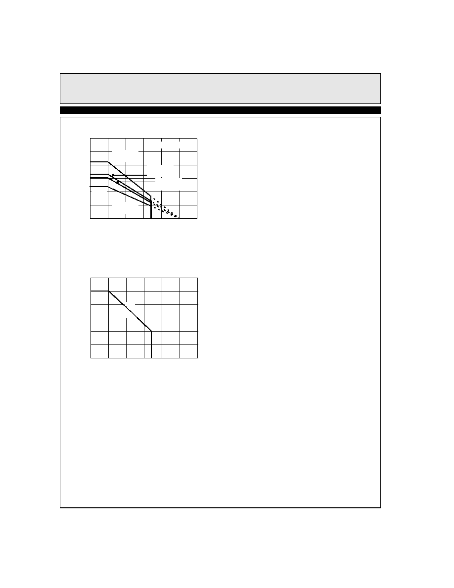
Figure 4. Package Power Dissipation vs
Ambient Temperature
Figure 5. Package Power Dissipation vs
Ambient Temperature
Unused Amplifiers
It is recommended that any unused amplifiers in a dual
and a quad package be configured as a unity gain fol-
lower. The inverting input should be directly connected
to the output and the non-inverting input tied to the
ground plane.
Driving Capacitive Loads
The EL5220C and EL5420C can drive a wide range of
capacitive loads. As load capacitance increases, how-
ever, the -3dB bandwidth of the device will decrease and
the peaking increase. The amplifiers drive 10pF loads in
parallel with 10k
with just 1.5dB of peaking, and
100pF with 6.4dB of peaking. If less peaking is desired
in these applications, a small series resistor (usually
between 5
and 50) can be placed in series with the
output. However, this will obviously reduce the gain
slightly. Another method of reducing peaking is to add a
“snubber” circuit at the output. A snubber is a shunt load
consisting of a resistor in series with a capacitor. Values
of 150
and 10nF are typical. The advantage of a snub-
ber is that it does not draw any DC load current or
reduce the gain
Power Supply Bypassing and Printed Circuit
Board Layout
The EL5220C and EL5420C can provide gain at high
frequency. As with any high-frequency device, good
printed circuit board layout is necessary for optimum
performance. Ground plane construction is highly rec-
ommended, lead lengths should be as short as possible
and the power supply pins must be well bypassed to
reduce the risk of oscillation. For normal single supply
operation, where the VS- pin is connected to ground, a
0.1F ceramic capacitor should be placed from VS+ to
pin to VS- pin. A 4.7F tantalum capacitor should then
be connected in parallel, placed in the region of the
amplifier. One 4.7F capacitor may be used for multiple
devices. This same capacitor combination should be
placed at each supply pin to ground if split supplies are
to be used.
MAX TJ=125°C
606mW
833mW
400
800
Po
w
er
Di
ss
ip
at
io
n
(m
W
)
Ambient Temperature (°C)
0
1200
1000
600
200
25
50
75
100
125
150
85
SO14
θJA=120°C/W
MSOP8
θJA=206°C/W
JEDEC JESD51-3 and SEMI G42-88 (Single Layer) Test
Board
667mW
485mW
TSSOP14
θJA=165°C/W
LPP16
θJA=150°C/W
JEDEC JESD51-7 High Effective Thermal Conductivity (4-
Layer) Test Board
(LPP exposed diepad soldered to PCB per JESD51-5)
3
2.5
2
1.5
1
0.5
0
25
50
75
100
125
150
Ambient Temperature (°C)
Po
w
er
Di
ss
ip
at
io
n
(W
)
85
2.500W
LPP
16
40°
C/W
相关PDF资料 |
PDF描述 |
|---|---|
| EL5420CL | 12MHz Rail-to-Rail Input-Output Op Amps |
| EL5420CL-T7 | 12MHz Rail-to-Rail Input-Output Op Amps |
| EL5420CR | 12MHz Rail-to-Rail Input-Output Op Amps |
| EL5420CS | 12MHz Rail-to-Rail Input-Output Op Amps |
| EL5420CS-T13 | 12MHz Rail-to-Rail Input-Output Op Amps |
相关代理商/技术参数 |
参数描述 |
|---|---|
| EL5420CRZ | 功能描述:高速运算放大器 EL5420CRZ 12MHZ QUAD RAIL INPUTOUTPUT OP RoHS:否 制造商:Texas Instruments 通道数量:1 电压增益 dB:116 dB 输入补偿电压:0.5 mV 转换速度:55 V/us 工作电源电压:36 V 电源电流:7.5 mA 最大工作温度:+ 85 C 安装风格:SMD/SMT 封装 / 箱体:SOIC-8 封装:Tube |
| EL5420CRZ-T13 | 功能描述:高速运算放大器 EL5420CRZ 12 MHZ QD R2R I/O OP RoHS:否 制造商:Texas Instruments 通道数量:1 电压增益 dB:116 dB 输入补偿电压:0.5 mV 转换速度:55 V/us 工作电源电压:36 V 电源电流:7.5 mA 最大工作温度:+ 85 C 安装风格:SMD/SMT 封装 / 箱体:SOIC-8 封装:Tube |
| EL5420CRZ-T7 | 功能描述:高速运算放大器 EL5420CRZ 12 MHZ QD R2R I/O OP RoHS:否 制造商:Texas Instruments 通道数量:1 电压增益 dB:116 dB 输入补偿电压:0.5 mV 转换速度:55 V/us 工作电源电压:36 V 电源电流:7.5 mA 最大工作温度:+ 85 C 安装风格:SMD/SMT 封装 / 箱体:SOIC-8 封装:Tube |
| EL5420CRZ-T7A | 功能描述:运算放大器 - 运放 EL5420CRZ 12 MHZ QD R2R I/O OP RoHS:否 制造商:STMicroelectronics 通道数量:4 共模抑制比(最小值):63 dB 输入补偿电压:1 mV 输入偏流(最大值):10 pA 工作电源电压:2.7 V to 5.5 V 安装风格:SMD/SMT 封装 / 箱体:QFN-16 转换速度:0.89 V/us 关闭:No 输出电流:55 mA 最大工作温度:+ 125 C 封装:Reel |
| EL5420CS | 功能描述:IC OPAMP QUAD R-R 12MHZ 14-SOIC RoHS:否 类别:集成电路 (IC) >> Linear - Amplifiers - Instrumentation 系列:- 标准包装:50 系列:LinCMOS™ 放大器类型:通用 电路数:4 输出类型:- 转换速率:0.05 V/µs 增益带宽积:110kHz -3db带宽:- 电流 - 输入偏压:0.7pA 电压 - 输入偏移:210µV 电流 - 电源:57µA 电流 - 输出 / 通道:30mA 电压 - 电源,单路/双路(±):3 V ~ 16 V,±1.5 V ~ 8 V 工作温度:-40°C ~ 85°C 安装类型:表面贴装 封装/外壳:14-SOIC(0.154",3.90mm 宽) 供应商设备封装:14-SOIC 包装:管件 产品目录页面:865 (CN2011-ZH PDF) 其它名称:296-1834296-1834-5 |
发布紧急采购,3分钟左右您将得到回复。