参数资料
| 型号: | EL5525IREZ-T13 |
| 厂商: | Intersil |
| 文件页数: | 8/10页 |
| 文件大小: | 0K |
| 描述: | IC VREF GEN 18CH TFTLCD 38HTSSOP |
| 标准包装: | 2,500 |
| 应用: | 转换器,TFT,LCD |
| 输入电压: | 4.5 V ~ 16.5 V |
| 输出数: | 18 |
| 输出电压: | 0.5 V ~ 14.95 V |
| 工作温度: | -40°C ~ 85°C |
| 安装类型: | 表面贴装 |
| 封装/外壳: | 38-TFSOP (0.173",4.40mm 宽)裸露焊盘 |
| 供应商设备封装: | 38-TSSOP 裸露焊盘 |
| 包装: | 带卷 (TR) |
�� �
�
�EL5525�
�takes� to� update� the� output� depends� on� the� timing� at� the� V� IN�
�and� the� state� of� the� switches.� It� can� take� 1� to� 18� clock� cycles�
�to� update� each� output.�
�For� the� sample� and� hold� capacitor� CH� to� maintain� the�
�correct� output� voltage,� the� driving� load� shouldn’t� be� changed�
�at� the� rising� edge� of� the� OSC� signal.� Since� at� the� rising� edge�
�of� the� OSC� clock,� the� refreshed� switches� are� being� opened,�
�if� the� load� changes� at� that� time,� it� will� generate� an� error�
�output� voltage.� For� a� fixed� load� condition,� the� internal�
�oscillator� can� be� used.�
�For� the� transient� load� condition,� the� external� OSC� mode�
�should� be� used� to� avoid� the� conflict� between� the� rising� edge�
�of� the� OSC� signal� and� the� changing� load.� So� a� timing� delay�
�circuit� will� be� needed� to� delay� the� OSC� signal� and� avoid� the�
�rising� edge� of� the� OSC� signal� and� changing� the� load� at� the�
�same� time.�
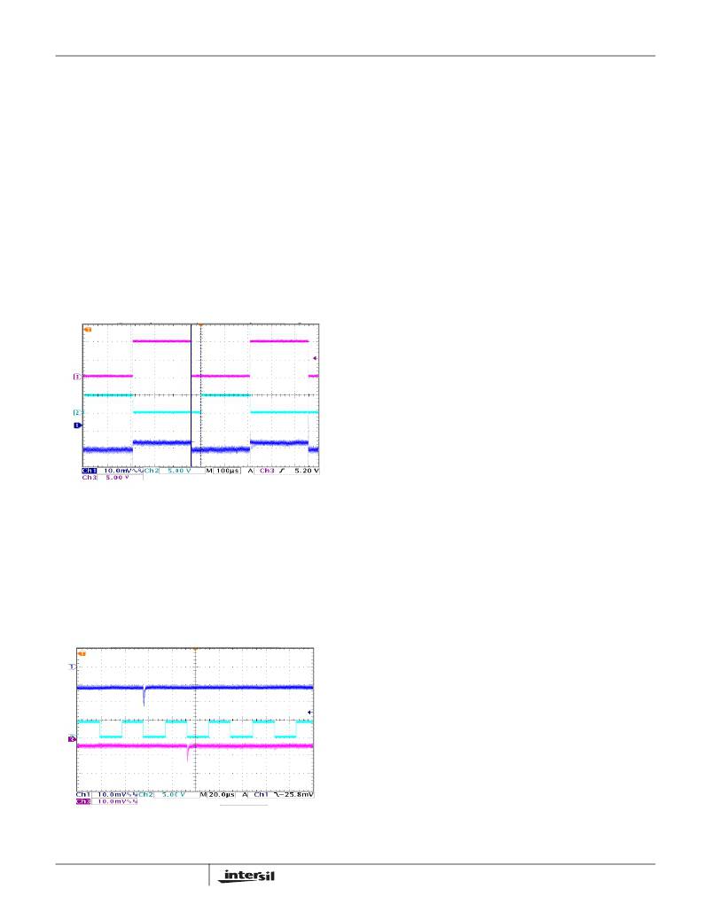
�Ch1� ---� Output1�
�Ch3� ---� Output2�
�Ch2� ---� EXT_OSC�
�At� the� falling� edge� of� the� OSC,� output� 1� is� being� refreshed,�
�and� one� clock� cycle� later,� output� 2� is� being� refreshed.� The�
�spike� you� see� here� is� the� response� of� the� output� amplifier�
�when� the� refreshed� switches� are� closed.� When� driving� a� big�
�capacitor� load,� there� will� be� ringing� at� the� spikes� because�
�the� phase� margin� of� the� amplifier� is� decreased.�
�The� speed� of� the� external� OSC� signal� shouldn’t� be� greater�
�than� 70kHz� because� for� the� worst� condition,� it� will� take� at�
�least� 4μs� to� charge� the� sample� and� hold� capacitor� CH.� The�
�pulse� width� has� to� be� at� least� 4μs� long.� From� our� lab� test,� the�
�duty� cycle� of� the� OSC� signal� must� be� greater� than� 30%.�
�POWER� DISSIPATION�
�With� the� 30mA� maximum� continues� output� drive� capability�
�for� each� channel,� it� is� possible� to� exceed� the� +125°C�
�absolute� maximum� junction� temperature.� Therefore,� it� is�
�important� to� calculate� the� maximum� junction� temperature� for�
�the� application� to� determine� if� load� conditions� need� to� be�
�modified� for� the� part� to� remain� in� the� safe� operation.�
�The� maximum� power� dissipation� allowed� in� a� package� is�
�determined� according� to:� Equation� 2:�
�Θ� JA�
�T� JMAX� -� T� AMAX�
�P� DMAX� =� ---------------------------------------------�
�(EQ.� 2)�
�FIGURE� 8.� TRANSIENT� LOAD� RESPONSE�
�Channel� 3� ---� sinking� and� sourcing� 5mA� current�
�Channel� 2� ---� EXT_OSC� signal�
�Channel� 1� ---� V� OUT�
�In� Figure� Table� 8� on� page� 8,� the� OSC� signal� is� synchronized�
�to� the� load� signal.� The� rising� edge� of� the� OSC� signal� is� then�
�delayed� by� some� amount� of� time� and� gives� enough� time� for�
�CH� to� be� charged� to� a� new� voltage� before� the� switches� are�
�where:�
�?� T� JMAX� =� Maximum� junction� temperature�
�?� T� AMAX� =� Maximum� ambient� temperature�
�?� θ� JA� =� Thermal� resistance� of� the� package�
�?� P� DMAX� =� Maximum� power� dissipation� in� the� package�
�The� maximum� power� dissipation� actually� produced� by� the� IC�
�is� the� total� quiescent� supply� current� times� the� total� power�
�supply� voltage� and� plus� the� power� in� the� IC� due� to� the� loads.�
�opened.�
�FIGURE� 9.� CHANNEL� TO� CHANNEL� REFRESH�
�8�
�P� DMAX� =� V� S� ×� I� S� +� Σ� [� (� V� S� -� V� OUT� i� )� ×� I� LOAD� i� ]�
�when� sourcing,� and:�
�P� DMAX� =� V� S� ×� I� S� +� Σ� (� V� OUT� i� ×� I� LOAD� i� )�
�when� sinking.�
�Where:�
�?� i� =� 18�
�?� V� S� =� Supply� voltage�
�?� I� S� =� Quiescent� current�
�?� V� OUT� i� =� Output� voltage� of� the� i� channel�
�?� I� LOAD� i� =� Load� current� of� the� i� channel�
�(EQ.� 3)�
�(EQ.� 4)�
�FN7393.2�
�September� 21,� 2010�
�相关PDF资料 |
PDF描述 |
|---|---|
| X40021V14-CT1 | IC VOLTAGE MONITOR DUAL 14-TSSOP |
| 160USC2200MEFCSN35X40 | CAP ALUM 2200UF 160V 20% SNAP-IN |
| ADP1715ARMZ-1.0-R7 | IC REG LDO 1V .5A 8-MSOP |
| ESM22DKKH | CONN EDGECARD 44POS .156 WW |
| RCM22DTAH-S189 | CONN EDGECARD 44POS R/A .156 SLD |
相关代理商/技术参数 |
参数描述 |
|---|---|
| EL5525IREZ-T7 | 功能描述:LCD Gamma缓冲器 EL5525IREZ 18-CH TFT LCDFERENCE VAGE GEN RoHS:否 制造商:Maxim Integrated 输入补偿电压: 转换速度: 电源电压-最大:20 V 电源电压-最小:9 V 电源电流: 最大功率耗散: 最大工作温度:+ 85 C 安装风格:SMD/SMT 封装 / 箱体:TQFN-38 封装:Tube |
| EL552-6 | 制造商:未知厂家 制造商全称:未知厂家 功能描述:Logic IC |
| EL552-7 | 制造商:未知厂家 制造商全称:未知厂家 功能描述:Logic IC |
| EL552-8 | 制造商:未知厂家 制造商全称:未知厂家 功能描述:Logic IC |
| EL552-9 | 制造商:未知厂家 制造商全称:未知厂家 功能描述:Logic IC |
发布紧急采购,3分钟左右您将得到回复。