参数资料
| 型号: | EL7586ILZ-T7 |
| 厂商: | Intersil |
| 文件页数: | 13/21页 |
| 文件大小: | 0K |
| 描述: | IC POWER SUPPLY TFT-LCD 20-QFN |
| 标准包装: | 1,000 |
| 应用: | 转换器,TFT,LCD |
| 输入电压: | 3 V ~ 5 V |
| 输出数: | 4 |
| 输出电压: | 5.5 V ~ 20 V |
| 工作温度: | -40°C ~ 85°C |
| 安装类型: | 表面贴装 |
| 封装/外壳: | 20-VFQFN 裸露焊盘 |
| 供应商设备封装: | 20-QFN 裸露焊盘(4x4) |
| 包装: | 带卷 (TR) |
�� �
�
�EL7586,� EL7586A�
�Operation� of� the� DELB� Output� Function�
�An� open� drain� DELB� output� is� provided� to� allow� the� boost�
�output� voltage,� developed� at� C� 2� (see� application� diagram),�
�to� be� delayed� via� an� external� switch� (Q4)� to� a� time� after� the�
�V� BOOST� supply� and� negative� V� OFF� charge� pump� supply�
�have� achieved� regulation� during� the� start-up� sequence�
�shown� in� Figures� 33� and� 34.� This� then� allows� the� A� VDD� and�
�V� ON� supplies� to� start-up� from� 0V� instead� of� the� normal� offset�
�voltage� of� V� IN� -V� DIODE� (D� 1� )� if� Q4� were� not� present.�
�When� DELB� is� activated� by� the� start-up� sequencer,� it� sinks�
�V� IN�
�EL7586�
�EL7586A�
�LX�
�FB�
�V� BOOST�
�50μA� allowing� a� controlled� turn-on� of� Q4� and� charge-up� of�
�C� 9� .� C� 16� can� be� used� to� control� the� turn-on� time� of� Q4� to�
�reduce� inrush� current� into� C� 9� .� The� potential� divider� formed�
�by� R� 9� and� R� 8� can� be� used� to� limit� the� V� GS� voltage� of� Q4� if�
�required� by� the� voltage� rating� of� this� device.� When� the�
�voltage� at� DELB� falls� to� less� than� 0.6V,� the� sink� current� is�
�increased� to� ~1.2mA� to� firmly� pull� DELB� to� 0V.�
�The� voltage� at� DELB� is� monitored� by� the� fault� protection�
�circuit� so� that� if� the� initial� 50μA� sink� current� fails� to� pull� DELB�
�below� ~0.6V� after� the� start-up� sequencing� has� completed,�
�then� a� fault� condition� will� be� detected� and� a� fault� time-out�
�ramp� will� be� initiated� on� the� C� DEL� capacitor� (C� 7� ).�
�Operation� of� the� PG� Output� Function�
�The� PG� output� consists� of� an� internal� pull-up� PMOS� device� to�
�V� IN� ,� to� turn-off� the� external� Q1� protection� switch� and� a� current�
�limited� pull-down� NMOS� device� which� sinks� ~15μA� allowing� a�
�controlled� turn-on� of� Q1� gate� capacitance.� C� O� is� used� to�
�control� how� fast� Q1� turns-on� -� limiting� inrush� current� into� C� 1� .�
�When� the� voltage� at� the� PG� pin� falls� to� less� than� 0.6V,� the� PG�
�sink� current� is� increased� to� ~1.2mA� to� firmly� pull� the� pin� to� 0V.�
�The� voltage� at� PG� is� monitored� by� the� fault� protection� circuit�
�so� that� if� the� initial� 15μA� sink� current� fails� to� pull� PG� below�
�~0.6V� after� the� start-up� sequencing� has� completed,� then� a�
�fault� condition� will� be� detected� and� a� fault� time-out� ramp� will�
�be� initiated� on� the� C� DEL� capacitor� (C� 7� ).�
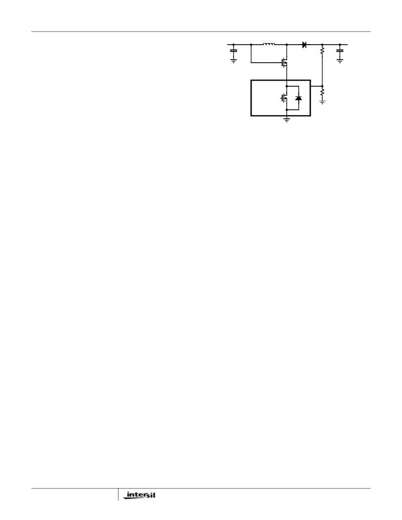
�Cascaded� MOSFET� Application�
�A� 20V� N-channel� MOSFET� is� integrated� in� the� boost�
�regulator.� For� the� applications� where� the� output� voltage� is�
�greater� than� 20V,� an� external� cascaded� MOSFET� is� needed�
�as� shown� in� Figure� 27.� The� voltage� rating� of� the� external�
�MOSFET� should� be� greater� than� V� BOOST� .�
�13�
�FIGURE� 27.� CASCADED� MOSFET� TOPOLOGY� FOR� HIGH�
�OUTPUT� VOLTAGE� APPLICATIONS�
�Linear-Regulator� Controllers� (V� ON� ,� V� LOGIC� ,� and�
�V� OFF� )�
�The� EL7586� and� EL7586A� include� three� independent� linear-�
�regulator� controllers,� in� which� two� are� positive� output� voltage�
�(V� ON� and� V� LOGIC� ),� and� one� is� negative.� The� V� ON� ,� V� OFF� ,�
�and� V� LOGIC� linear-regulator� controller� functional� diagrams,�
�applications� circuits� are� shown� in� Figures� 28,� 29,� and� 30�
�respectively.�
�Calculation� of� the� Linear� Regulator� Base-Emitter�
�Resistors� (R� BL� ,� R� BP� and� R� BN� )�
�For� the� pass� transistor� of� the� linear� regulator,� low� frequency�
�gain� (Hfe)� and� unity� gain� freq.� (f� T� )� are� usually� specified� in� the�
�datasheet.� The� pass� transistor� adds� a� pole� to� the� loop�
�transfer� function� at� f� p� =� f� T� /Hfe.� Therefore,� in� order� to�
�maintain� phase� margin� at� low� frequency,� the� best� choice� for�
�a� pass� device� is� often� a� high� frequency� low� gain� switching�
�transistor.� Further� improvement� can� be� obtained� by� adding� a�
�base-emitter� resistor� R� BE� (R� BP� ,� R� BL� ,� R� BN� in� the� Functional�
�Block� Diagram),� which� increase� the� pole� frequency� to:�
�f� p� =� f� T� *(1+� Hfe� *re/R� BE� )/Hfe,� where� re� =� KT/qIc.� So� choose�
�the� lowest� value� R� BE� in� the� design� as� long� as� there� is� still�
�enough� base� current� (I� B� )� to� support� the� maximum� output�
�current� (I� C� ).�
�We� will� take� as� an� example� the� V� LOGIC� linear� regulator.� If� a�
�Fairchild� FMMT549� PNP� transistor� is� used� as� the� external�
�pass� transistor,� Q5� in� the� application� diagram,� then� for� a�
�maximum� V� LOGIC� operating� requirement� of� 500mA� the� data�
�sheet� indicates� Hfe_min� =� 100.�
�The� base-emitter� saturation� voltage� is:� Vbe_max� =� 1.25V�
�(note� this� is� normally� a� Vbe� ~� 0.7V,� however,� for� the� Q5�
�transistor� an� internal� Darlington� arrangement� is� used� to�
�increase� it's� current� gain,� giving� a� 'base-emitter'� voltage� of�
�2� x� V� BE� ).�
�(Note� that� using� a� high� current� Darlington� PNP� transistor� for�
�Q5� requires� that� V� IN� >� V� LOGIC� +� 2V.� Should� a� lower� input�
�voltage� be� required,� then� an� ordinary� high� gain� PNP�
�transistor� should� be� selected� for� Q5� so� as� to� allow� a� lower�
�collector-emitter� saturation� voltage).�
�FN9210.2�
�January� 17,� 2006�
�相关PDF资料 |
PDF描述 |
|---|---|
| GMC50DREI-S13 | CONN EDGECARD 100POS .100 EXTEND |
| EMM24DRMD | CONN EDGECARD 48POS .156 WW |
| EL7586ILZ-T13 | IC POWER SUPPLY TFT-LCD 20-QFN |
| EMM24DRKS | CONN EDGECARD 48POS DIP .156 SLD |
| EL7586AILZ-T7 | IC POWER SUPPLY TFT-LCD 20-QFN |
相关代理商/技术参数 |
参数描述 |
|---|---|
| EL7630 | 制造商:INTERSIL 制造商全称:Intersil Corporation 功能描述:White LED Boost Regulator |
| EL7630_06 | 制造商:INTERSIL 制造商全称:Intersil Corporation 功能描述:White LED Boost Regulator |
| EL7630ICZ | 制造商:Intersil Corporation 功能描述:LED DRVR 6SEGMENT 2.7V TO 5.5V 6PIN SC-70 - Bulk |
| EL7630ICZ-T7 | 功能描述:LED显示驱动器 EL7630ICZ WHT LED BOOSTG RoHS:否 制造商:Micrel 数位数量:5 片段数量: 安装风格:SMD/SMT 封装 / 箱体:PLCC-44 工作电源电压:4.75 V to 11 V 最大电源电流:10 mA 最大工作温度:+ 85 C 最小工作温度:- 40 C 封装:Tube |
| EL7630ICZ-T7A | 功能描述:LED显示驱动器 EL7630ICZ WHT LED BOOSTG RoHS:否 制造商:Micrel 数位数量:5 片段数量: 安装风格:SMD/SMT 封装 / 箱体:PLCC-44 工作电源电压:4.75 V to 11 V 最大电源电流:10 mA 最大工作温度:+ 85 C 最小工作温度:- 40 C 封装:Tube |
发布紧急采购,3分钟左右您将得到回复。