参数资料
| 型号: | EL8200IYZ-T13 |
| 厂商: | Intersil |
| 文件页数: | 3/15页 |
| 文件大小: | 0K |
| 描述: | IC AMP DUAL R-R 200MHZ 10-MSOP |
| 标准包装: | 2,500 |
| 放大器类型: | 电压反馈 |
| 电路数: | 2 |
| 输出类型: | 满摆幅 |
| 转换速率: | 200 V/µs |
| 增益带宽积: | 100MHz |
| -3db带宽: | 200MHz |
| 电流 - 输入偏压: | 1.6µA |
| 电压 - 输入偏移: | 800µV |
| 电流 - 电源: | 2mA |
| 电流 - 输出 / 通道: | 65mA |
| 电压 - 电源,单路/双路(±): | 3 V ~ 5 V,±1.5 V ~ 2.5 V |
| 工作温度: | -40°C ~ 85°C |
| 安装类型: | 表面贴装 |
| 封装/外壳: | 10-TFSOP,10-MSOP(0.118",3.00mm 宽) |
| 供应商设备封装: | 10-MSOP |
| 包装: | 带卷 (TR) |
11
FN7105.3
August 29, 2007
dissipation could easily increase such that the part will be
destroyed. Maximum reliability is maintained if the output
current never exceeds ±40mA. This limit is set by the design
of the internal metal interconnections.
Power Dissipation
With the high output drive capability of the EL8200, EL8201
and EL8401, it is possible to exceed the 125
°C absolute
maximum junction temperature under certain load current
conditions. Therefore, it is important to calculate the
maximum junction temperature for the application to
determine if the load conditions or package types need to be
modified for the amplifier to remain in the safe operating
area.
The maximum power dissipation allowed in a package is
determined according to:
Where:
TJMAX = Maximum junction temperature
TAMAX = Maximum ambient temperature
θ
JA = Thermal resistance of the package
The maximum power dissipation actually produced by an IC
is the total quiescent supply current times the total power
supply voltage, plus the power in the IC due to the load, or:
For sourcing:
For sinking:
Where:
VS = Total supply voltage
ISMAX = Maximum quiescent supply current
VOUTi = Maximum output voltage of the application for
each channel
RLOADi = Load resistance tied to ground for each channel
ILOADi = Load current for each channel
By setting the two PDMAX equations equal to each other, we
can solve the output current and RLOADi to avoid the device
overheat.
Power Supply Bypassing and Printed Circuit
Board Layout
As with any high frequency device, a good printed circuit
board layout is necessary for optimum performance. Lead
lengths should be as sort as possible. The power supply pin
must be well bypassed to reduce the risk of oscillation. For
normal single supply operation, where the VS- pin is
connected to the ground plane, a single 4.7F tantalum
capacitor in parallel with a 0.1F ceramic capacitor from VS+
to GND will suffice. This same capacitor combination should
be placed at each supply pin to ground if split supplies are to
be used. In this case, the VS- pin becomes the negative
supply rail.
For good AC performance, parasitic capacitance should be
kept to a minimum. Use of wire wound resistors should be
avoided because of their additional series inductance. Use
of sockets should also be avoided if possible. Sockets add
parasitic inductance and capacitance that can result in
compromised performance. Minimizing parasitic capacitance
at the amplifier’s inverting input pin is very important. The
feedback resistor should be placed very close to the
inverting input pin. Strip line design techniques are
recommended for the signal traces.
Typical Applications
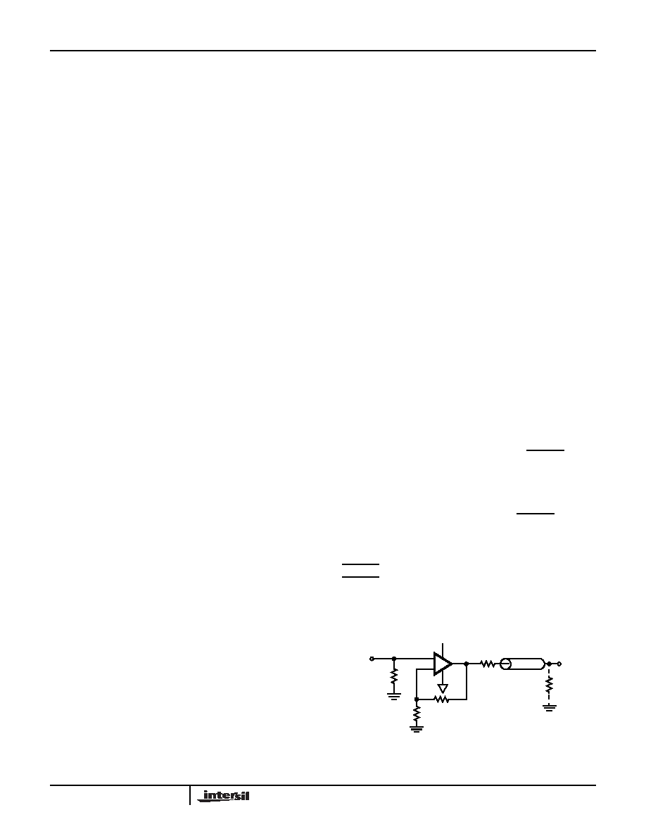
VIDEO SYNC PULSE REMOVER
Many CMOS analog to digital converters have a parasitic
latch up problem when subjected to negative input voltage
levels. Since the sync tip contains no useful video
information and it is a negative going pulse, we can chop it
shows the complete input video signal applied at the input,
as well as the output signal with the negative going sync
pulse removed.
MULTIPLEXER
Besides the normal power down usage, the ENABLE pin of
the EL8200 can be used for multiplexing applications.
Figure 31 shows two channels with the outputs tied together,
driving a back terminated 75
Ω video load. A 2V
P-P 2MHz
sine wave is applied to Amp A and a 1VP-P 2MHz sine wave
is applied to Amp B. Figure 32 shows the ENABLE signal
and the resulting output waveform at VOUT. Observe the
break-before-make operation of the multiplexing. Amp A is
on and VIN1 is passed through to the output when the
ENABLE signal is low and turns off in about 25ns when the
ENABLE signal is high. About 200ns later, Amp B turns on
and VIN2 is passed through to the output. The break-before-
make operation ensures that more than one amplifier isn’t
trying to drive the bus at the same time.
PD
MAX
T
JMAX
T
AMAX
–
θ
JA
---------------------------------------------
=
PD
MAX
V
S
I
SMAX
Σ V
S
V
OUTi
–
()
V
OUTi
R
Li
-----------------
×
+
×
=
PD
MAX
V
S
I
SMAX
Σ V
OUTi
V
S-
–
() I
LOADi
×
+
×
=
FIGURE 29. SYNC PULSE REMOVER
5V
1K
VOUT
VIN
75
Ω
+
-
75
Ω
1K
75
Ω
VS+
VS-
EL8200, EL8201, EL8401
相关PDF资料 |
PDF描述 |
|---|---|
| N3433-5602 | CONN HEADER 50POS R/A LONG LATCH |
| 961254-6300-AR-TP | CONN HEADER STR DL 54PS GOLD SMD |
| 521293-1 | CONN RECEPT 16-18AWG 0.187 NATRL |
| TSW-150-06-G-S | CONN HEADER 50POS .100" SGL GOLD |
| 208456015001169 | CONNECTOR RECEPT 15POS |
相关代理商/技术参数 |
参数描述 |
|---|---|
| EL8200IYZ-T7 | 功能描述:运算放大器 - 运放 EL8200IYZ DL 200 MHZ RAIL-TO-RAIL AMP RoHS:否 制造商:STMicroelectronics 通道数量:4 共模抑制比(最小值):63 dB 输入补偿电压:1 mV 输入偏流(最大值):10 pA 工作电源电压:2.7 V to 5.5 V 安装风格:SMD/SMT 封装 / 箱体:QFN-16 转换速度:0.89 V/us 关闭:No 输出电流:55 mA 最大工作温度:+ 125 C 封装:Reel |
| EL8201 | 制造商:INTERSIL 制造商全称:Intersil Corporation 功能描述:200MHz Rail-to-Rail Amplifiers |
| EL8201IS | 功能描述:IC OP AMP 200MHZ R-R 8-SOIC RoHS:否 类别:集成电路 (IC) >> Linear - Amplifiers - Instrumentation 系列:- 标准包装:1,000 系列:- 放大器类型:电压反馈 电路数:4 输出类型:满摆幅 转换速率:33 V/µs 增益带宽积:20MHz -3db带宽:30MHz 电流 - 输入偏压:2nA 电压 - 输入偏移:3000µV 电流 - 电源:2.5mA 电流 - 输出 / 通道:30mA 电压 - 电源,单路/双路(±):4.5 V ~ 16.5 V,±2.25 V ~ 8.25 V 工作温度:-40°C ~ 85°C 安装类型:表面贴装 封装/外壳:14-SOIC(0.154",3.90mm 宽) 供应商设备封装:14-SOIC 包装:带卷 (TR) |
| EL8201IS-T13 | 功能描述:IC AMP DUAL R-R 200MHZ 8-SOIC RoHS:否 类别:集成电路 (IC) >> Linear - Amplifiers - Instrumentation 系列:- 标准包装:50 系列:LinCMOS™ 放大器类型:通用 电路数:4 输出类型:- 转换速率:0.05 V/µs 增益带宽积:110kHz -3db带宽:- 电流 - 输入偏压:0.7pA 电压 - 输入偏移:210µV 电流 - 电源:57µA 电流 - 输出 / 通道:30mA 电压 - 电源,单路/双路(±):3 V ~ 16 V,±1.5 V ~ 8 V 工作温度:-40°C ~ 85°C 安装类型:表面贴装 封装/外壳:14-SOIC(0.154",3.90mm 宽) 供应商设备封装:14-SOIC 包装:管件 产品目录页面:865 (CN2011-ZH PDF) 其它名称:296-1834296-1834-5 |
| EL8201IS-T7 | 功能描述:IC OP AMP 200MHZ R-R 8-SOIC RoHS:否 类别:集成电路 (IC) >> Linear - Amplifiers - Instrumentation 系列:- 标准包装:50 系列:- 放大器类型:通用 电路数:2 输出类型:满摆幅 转换速率:1.8 V/µs 增益带宽积:6.5MHz -3db带宽:4.5MHz 电流 - 输入偏压:5nA 电压 - 输入偏移:100µV 电流 - 电源:65µA 电流 - 输出 / 通道:35mA 电压 - 电源,单路/双路(±):1.8 V ~ 5.25 V,±0.9 V ~ 2.625 V 工作温度:-40°C ~ 85°C 安装类型:表面贴装 封装/外壳:10-TFSOP,10-MSOP(0.118",3.00mm 宽) 供应商设备封装:10-MSOP 包装:管件 |
发布紧急采购,3分钟左右您将得到回复。