- 您现在的位置:买卖IC网 > PDF目录11581 > ENC424J600T-I/PT (Microchip Technology)IC ETHERNET CTRLR W/SPI 44-TQFP PDF资料下载
参数资料
| 型号: | ENC424J600T-I/PT |
| 厂商: | Microchip Technology |
| 文件页数: | 2/168页 |
| 文件大小: | 0K |
| 描述: | IC ETHERNET CTRLR W/SPI 44-TQFP |
| 视频文件: | Fast 100 Mbps Ethernet PICtail Plus Overview |
| 标准包装: | 1,200 |
| 控制器类型: | 以太网控制器(IEEE 802.3) |
| 接口: | SPI |
| 电源电压: | 3 V ~ 3.6 V |
| 电流 - 电源: | 96mA |
| 工作温度: | -40°C ~ 85°C |
| 安装类型: | 表面贴装 |
| 封装/外壳: | 44-TQFP |
| 供应商设备封装: | 44-TQFP(10x10) |
| 包装: | 带卷 (TR) |
| 配用: | AC164132-ND - BOARD DAUGHTER PICTAIL ETHERNET |
第1页当前第2页第3页第4页第5页第6页第7页第8页第9页第10页第11页第12页第13页第14页第15页第16页第17页第18页第19页第20页第21页第22页第23页第24页第25页第26页第27页第28页第29页第30页第31页第32页第33页第34页第35页第36页第37页第38页第39页第40页第41页第42页第43页第44页第45页第46页第47页第48页第49页第50页第51页第52页第53页第54页第55页第56页第57页第58页第59页第60页第61页第62页第63页第64页第65页第66页第67页第68页第69页第70页第71页第72页第73页第74页第75页第76页第77页第78页第79页第80页第81页第82页第83页第84页第85页第86页第87页第88页第89页第90页第91页第92页第93页第94页第95页第96页第97页第98页第99页第100页第101页第102页第103页第104页第105页第106页第107页第108页第109页第110页第111页第112页第113页第114页第115页第116页第117页第118页第119页第120页第121页第122页第123页第124页第125页第126页第127页第128页第129页第130页第131页第132页第133页第134页第135页第136页第137页第138页第139页第140页第141页第142页第143页第144页第145页第146页第147页第148页第149页第150页第151页第152页第153页第154页第155页第156页第157页第158页第159页第160页第161页第162页第163页第164页第165页第166页第167页第168页
ENC424J600/624J600
DS39935C-page 8
2010 Microchip Technology Inc.
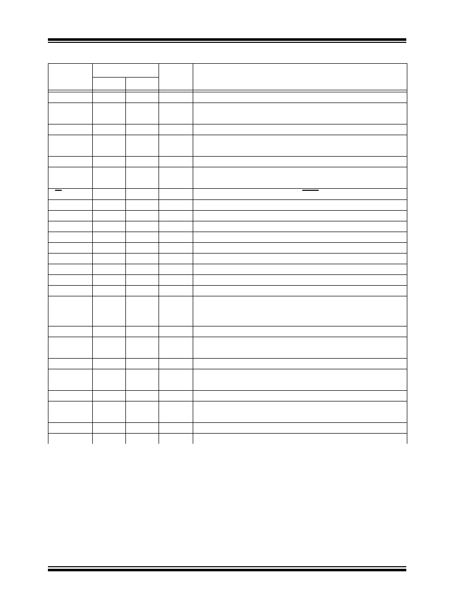
OSC1
3
I
ANA
25 MHz Crystal Oscillator/Clock Input
OSC2
2
O
—
25 MHz Crystal Oscillator Output
PSPCFG0
32
—
I
CMOS
PSP Mode Select 0
PSPCFG1
—
45
I
CMOS
PSP Mode Select 1
PSPCFG2
—
17
I
CMOS
PSP Mode Select 2
PSPCFG3
—
18
I
CMOS
PSP Mode Select 3
PSPCFG4
—
52
I
CMOS
PSP Mode Select 4
RBIAS
11
16
I
ANA
PHY Bias (external resistor) Connection
RD
36
51
I
CMOS
PSP Read Strobe
RW
36
51
I
CMOS
PSP Combined Read/Write Signal
SCK
37
52
I
CMOS
SPI Serial Clock Input
SI
36
51
I
CMOS
SPI Serial Data Input (from Master)
SO
35
50
O
—
SPI Serial Data Out (to Master)
SPISEL
24
34
I
CMOS
SPI/PSP Interface Select
TPIN-
17
27
I
ANA
Differential Ethernet Receive Minus Signal Input
TPIN+
16
26
I
ANA
Differential Ethernet Receive Plus Signal Input
TPOUT-
21
31
O
—
Differential Ethernet Transmit Minus Signal Output
TPOUT+
20
30
O
—
Differential Ethernet Transmit Plus Signal Output
VCAP
43
63
P
—
Regulator External Capacitor connection
VDD
44
21, 47,
64
P
—
Positive 3.3V Power Supply for Digital Logic
VDDOSC
4
P
—
Positive 3.3V Power Supply for 25 MHz Oscillator
VDDPLL
12
22
P
—
Positive 3.3V Power Supply for PHY PLL Circuitry
VDDRX
15
25
P
—
Positive 3.3V Power Supply for PHY RX Circuitry
VDDTX
18
28
P
—
Positive 3.3V Power Supply for PHY TX Circuitry
VSS
33, 42
46, 62
P
—
Ground Reference for Digital Logic
VSSOSC
1
P
—
Ground Reference for 25 MHz Oscillator
VSSPLL
13
23
P
—
Ground Reference for PHY PLL Circuitry
VSSRX
14
24
P
—
Ground Reference for PHY RX Circuitry
VSSTX
19, 22
29, 32
P
—
Ground Reference for PHY TX Circuitry
WR
35
50
I
CMOS
PSP Write Strobe
WRH
—
48
I
CMOS
PSP Write High Strobe
WRL
—
50
I
CMOS
PSP Write Low Strobe
TABLE 1-2:
ENC424J600/624J600 PINOUT DESCRIPTIONS (CONTINUED)
Pin Name
Pin Number
Pin Type
Input
Buffer
Description
44-Pin
64-Pin
Legend: I = Input; O = Output; P = Power; CMOS = CMOS compatible input buffer; ANA = Analog level input/output
相关PDF资料 |
PDF描述 |
|---|---|
| PIC16LC505T-04I/SL | IC MCU OTP 1KX12 14SOIC |
| PIC16C620A-04/SS | IC MCU OTP 512X14 COMP 20SSOP |
| PIC16C620A-04I/SS | IC MCU OTP 512X14 COMP 20SSOP |
| PIC12LCE519T-04/SM | IC MCU OTP 1KX12 LV W/EE 8-SOIJ |
| MCP2510T-I/ST | IC CAN CONTROLLER W/SPI 20-TSSOP |
相关代理商/技术参数 |
参数描述 |
|---|---|
| ENC431D05A | 制造商:未知厂家 制造商全称:未知厂家 功能描述: |
| ENC431D-05A | 制造商:未知厂家 制造商全称:未知厂家 功能描述:STD MOV |
| ENC431D07A | 制造商:未知厂家 制造商全称:未知厂家 功能描述: |
| ENC431D-07A | 制造商:未知厂家 制造商全称:未知厂家 功能描述:STD MOV |
| ENC431D10A | 制造商:未知厂家 制造商全称:未知厂家 功能描述: |
发布紧急采购,3分钟左右您将得到回复。