参数资料
| 型号: | EP1K10FC256-2N |
| 厂商: | Altera |
| 文件页数: | 21/86页 |
| 文件大小: | 0K |
| 描述: | IC ACEX 1K FPGA 10K 256-FBGA |
| 产品培训模块: | Three Reasons to Use FPGA's in Industrial Designs |
| 标准包装: | 90 |
| 系列: | ACEX-1K® |
| LAB/CLB数: | 72 |
| 逻辑元件/单元数: | 576 |
| RAM 位总计: | 12288 |
| 输入/输出数: | 136 |
| 门数: | 56000 |
| 电源电压: | 2.375 V ~ 2.625 V |
| 安装类型: | 表面贴装 |
| 工作温度: | 0°C ~ 85°C |
| 封装/外壳: | 256-BGA |
| 供应商设备封装: | 256-FBGA(17x17) |
第1页第2页第3页第4页第5页第6页第7页第8页第9页第10页第11页第12页第13页第14页第15页第16页第17页第18页第19页第20页当前第21页第22页第23页第24页第25页第26页第27页第28页第29页第30页第31页第32页第33页第34页第35页第36页第37页第38页第39页第40页第41页第42页第43页第44页第45页第46页第47页第48页第49页第50页第51页第52页第53页第54页第55页第56页第57页第58页第59页第60页第61页第62页第63页第64页第65页第66页第67页第68页第69页第70页第71页第72页第73页第74页第75页第76页第77页第78页第79页第80页第81页第82页第83页第84页第85页第86页
28
Altera Corporation
ACEX 1K Programmable Logic Device Family Data Sheet
For improved routing, the row interconnect consists of a combination of
full-length and half-length channels. The full-length channels connect to
all LABs in a row; the half-length channels connect to the LABs in half of
the row. The EAB can be driven by the half-length channels in the left half
of the row and by the full-length channels. The EAB drives out to the full-
length channels. In addition to providing a predictable, row-wide
interconnect, this architecture provides increased routing resources. Two
neighboring LABs can be connected using a half-row channel, thereby
saving the other half of the channel for the other half of the row.
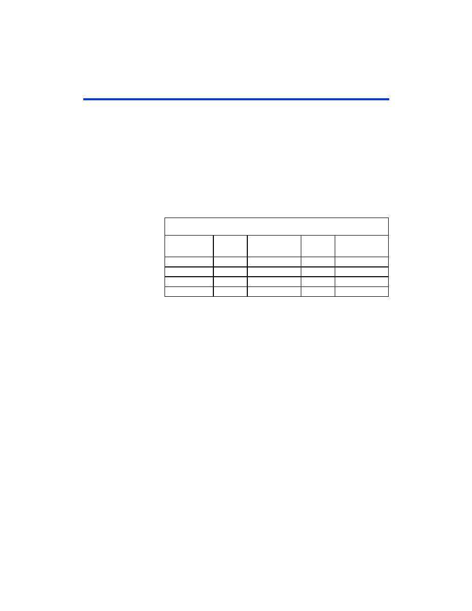
Table 6 summarizes the FastTrack Interconnect routing structure
resources available in each ACEX 1K device.
In addition to general-purpose I/O pins, ACEX 1K devices have six
dedicated input pins that provide low-skew signal distribution across the
device. These six inputs can be used for global clock, clear, preset, and
peripheral output-enable and clock-enable control signals. These signals
are available as control signals for all LABs and IOEs in the device. The
dedicated inputs can also be used as general-purpose data inputs because
they can feed the local interconnect of each LAB in the device.
Figure 14 shows the interconnection of adjacent LABs and EABs, with
row, column, and local interconnects, as well as the associated cascade
and carry chains. Each LAB is labeled according to its location: a letter
represents the row and a number represents the column. For example,
LAB B3 is in row B, column 3.
Table 6. ACEX 1K FastTrack Interconnect Resources
Device
Rows
Channels per
Row
Columns
Channels per
Column
EP1K10
3
144
24
EP1K30
6
216
36
24
EP1K50
10
216
36
24
EP1K100
12
312
52
24
相关PDF资料 |
PDF描述 |
|---|---|
| A3P125-2FG144I | IC FPGA 1KB FLASH 125K 144-FBGA |
| A3P125-2FGG144I | IC FPGA 1KB FLASH 125K 144-FBGA |
| BR25S320FV-WE2 | IC EEPROM SPI 32KB 20MHZ 8-SSOP |
| EX64-PTQ64I | IC FPGA ANTIFUSE 3K 64-TQFP |
| EX64-PTQG64I | IC FPGA ANTIFUSE 3K 64-TQFP |
相关代理商/技术参数 |
参数描述 |
|---|---|
| EP1K10FC256-3 | 功能描述:FPGA - 现场可编程门阵列 FPGA - ACEX 1K 72 LABs 136 IOs RoHS:否 制造商:Altera Corporation 系列:Cyclone V E 栅极数量: 逻辑块数量:943 内嵌式块RAM - EBR:1956 kbit 输入/输出端数量:128 最大工作频率:800 MHz 工作电源电压:1.1 V 最大工作温度:+ 70 C 安装风格:SMD/SMT 封装 / 箱体:FBGA-256 |
| EP1K10FC256-3N | 功能描述:FPGA - 现场可编程门阵列 FPGA - ACEX 1K 72 LABs 136 IOs RoHS:否 制造商:Altera Corporation 系列:Cyclone V E 栅极数量: 逻辑块数量:943 内嵌式块RAM - EBR:1956 kbit 输入/输出端数量:128 最大工作频率:800 MHz 工作电源电压:1.1 V 最大工作温度:+ 70 C 安装风格:SMD/SMT 封装 / 箱体:FBGA-256 |
| EP1K10FI256-2 | 功能描述:FPGA - 现场可编程门阵列 FPGA - ACEX 1K 72 LABs 136 IOs RoHS:否 制造商:Altera Corporation 系列:Cyclone V E 栅极数量: 逻辑块数量:943 内嵌式块RAM - EBR:1956 kbit 输入/输出端数量:128 最大工作频率:800 MHz 工作电源电压:1.1 V 最大工作温度:+ 70 C 安装风格:SMD/SMT 封装 / 箱体:FBGA-256 |
| EP1K10FI256-2N | 功能描述:FPGA - 现场可编程门阵列 FPGA - ACEX 1K 72 LABs 136 IOs RoHS:否 制造商:Altera Corporation 系列:Cyclone V E 栅极数量: 逻辑块数量:943 内嵌式块RAM - EBR:1956 kbit 输入/输出端数量:128 最大工作频率:800 MHz 工作电源电压:1.1 V 最大工作温度:+ 70 C 安装风格:SMD/SMT 封装 / 箱体:FBGA-256 |
| EP1K10QC208-1 | 功能描述:FPGA - 现场可编程门阵列 FPGA - ACEX 1K 72 LABs 120 IOs RoHS:否 制造商:Altera Corporation 系列:Cyclone V E 栅极数量: 逻辑块数量:943 内嵌式块RAM - EBR:1956 kbit 输入/输出端数量:128 最大工作频率:800 MHz 工作电源电压:1.1 V 最大工作温度:+ 70 C 安装风格:SMD/SMT 封装 / 箱体:FBGA-256 |
发布紧急采购,3分钟左右您将得到回复。