- 您现在的位置:买卖IC网 > PDF目录19361 > EP1K30FC256-3 (Altera)IC ACEX 1K FPGA 30K 256-FBGA PDF资料下载
参数资料
| 型号: | EP1K30FC256-3 |
| 厂商: | Altera |
| 文件页数: | 11/86页 |
| 文件大小: | 0K |
| 描述: | IC ACEX 1K FPGA 30K 256-FBGA |
| 产品培训模块: | Three Reasons to Use FPGA's in Industrial Designs |
| 标准包装: | 90 |
| 系列: | ACEX-1K® |
| LAB/CLB数: | 216 |
| 逻辑元件/单元数: | 1728 |
| RAM 位总计: | 24576 |
| 输入/输出数: | 171 |
| 门数: | 119000 |
| 电源电压: | 2.375 V ~ 2.625 V |
| 安装类型: | 表面贴装 |
| 工作温度: | 0°C ~ 70°C |
| 封装/外壳: | 256-BGA |
| 供应商设备封装: | 256-FBGA(17x17) |
| 产品目录页面: | 602 (CN2011-ZH PDF) |
| 其它名称: | 544-1029 |
第1页第2页第3页第4页第5页第6页第7页第8页第9页第10页当前第11页第12页第13页第14页第15页第16页第17页第18页第19页第20页第21页第22页第23页第24页第25页第26页第27页第28页第29页第30页第31页第32页第33页第34页第35页第36页第37页第38页第39页第40页第41页第42页第43页第44页第45页第46页第47页第48页第49页第50页第51页第52页第53页第54页第55页第56页第57页第58页第59页第60页第61页第62页第63页第64页第65页第66页第67页第68页第69页第70页第71页第72页第73页第74页第75页第76页第77页第78页第79页第80页第81页第82页第83页第84页第85页第86页
Altera Corporation
19
ACEX 1K Programmable Logic Device Family Data Sheet
D
e
ve
lo
pm
e
n
t
13
To
o
ls
Cascade Chain
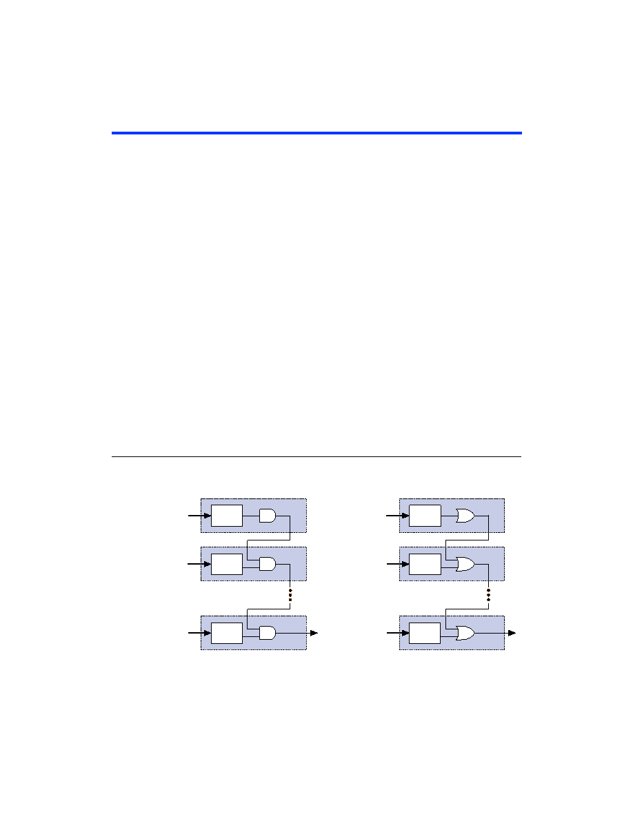
With the cascade chain, the ACEX 1K architecture can implement
functions that have a very wide fan-in. Adjacent LUTs can be used to
compute portions of the function in parallel; the cascade chain serially
connects the intermediate values. The cascade chain can use a logical AND
or logical OR (via De Morgan’s inversion) to connect the outputs of
adjacent LEs. With a delay as low as 0.6 ns per LE, each additional LE
provides four more inputs to the effective width of a function. Cascade
chain logic can be created automatically by the compiler during design
processing, or manually by the designer during design entry.
Cascade chains longer than eight bits are implemented automatically by
linking several LABs together. For easier routing, a long cascade chain
skips every other LAB in a row. A cascade chain longer than one LAB
skips either from even-numbered LAB to even-numbered LAB, or from
odd-numbered LAB to odd-numbered LAB (e.g., the last LE of the first
LAB in a row cascades to the first LE of the third LAB). The cascade chain
does not cross the center of the row (e.g., in the EP1K50 device, the cascade
chain stops at the eighteenth LAB, and a new one begins at the nineteenth
LAB). This break is due to the EAB’s placement in the middle of the row.
Figure 10 shows how the cascade function can connect adjacent LEs to
form functions with a wide fan-in. These examples show functions of 4n
variables implemented with n LEs. The LE delay is 1.3 ns; the cascade
chain delay is 0.6 ns. With the cascade chain, decoding a 16-bit address
requires 3.1 ns.
Figure 10. ACEX 1K Cascade Chain Operation
LE1
LUT
LE2
LUT
d[3..0]
d[7..4]
d[(4
n – 1)..(4n – 4)]
d[3..0]
d[7..4]
LE
n
LE1
LE2
LE
n
LUT
AND Cascade Chain
OR Cascade Chain
d[(4
n – 1)..(4n – 4)]
相关PDF资料 |
PDF描述 |
|---|---|
| MAX6692MSA+ | IC SENSOR REMOTE SMBUS 8SOIC |
| RGF1M | DIODE GPP FAST 1A 1000V SMA |
| DSP56321VL200 | IC DSP 24BIT 200MHZ 196-MAPBGA |
| AGM30DRSN-S288 | CONN EDGECARD EXTEND 60POS .156 |
| IRS2168DPBF | IC PFC BALLAST CTLR ADV 16-PDIP |
相关代理商/技术参数 |
参数描述 |
|---|---|
| EP1K30FC256-3N | 功能描述:FPGA - 现场可编程门阵列 FPGA - ACEX 1K 216 LABs 171 IOs RoHS:否 制造商:Altera Corporation 系列:Cyclone V E 栅极数量: 逻辑块数量:943 内嵌式块RAM - EBR:1956 kbit 输入/输出端数量:128 最大工作频率:800 MHz 工作电源电压:1.1 V 最大工作温度:+ 70 C 安装风格:SMD/SMT 封装 / 箱体:FBGA-256 |
| EP1K30FI256-2 | 功能描述:FPGA - 现场可编程门阵列 FPGA - ACEX 1K 216 LABs 171 IOs RoHS:否 制造商:Altera Corporation 系列:Cyclone V E 栅极数量: 逻辑块数量:943 内嵌式块RAM - EBR:1956 kbit 输入/输出端数量:128 最大工作频率:800 MHz 工作电源电压:1.1 V 最大工作温度:+ 70 C 安装风格:SMD/SMT 封装 / 箱体:FBGA-256 |
| EP1K30FI256-2N | 功能描述:FPGA - 现场可编程门阵列 FPGA - ACEX 1K 216 LABs 171 IOs RoHS:否 制造商:Altera Corporation 系列:Cyclone V E 栅极数量: 逻辑块数量:943 内嵌式块RAM - EBR:1956 kbit 输入/输出端数量:128 最大工作频率:800 MHz 工作电源电压:1.1 V 最大工作温度:+ 70 C 安装风格:SMD/SMT 封装 / 箱体:FBGA-256 |
| EP1K30QC208-1 | 功能描述:FPGA - 现场可编程门阵列 FPGA - ACEX 1K 216 LABs 147 IOs RoHS:否 制造商:Altera Corporation 系列:Cyclone V E 栅极数量: 逻辑块数量:943 内嵌式块RAM - EBR:1956 kbit 输入/输出端数量:128 最大工作频率:800 MHz 工作电源电压:1.1 V 最大工作温度:+ 70 C 安装风格:SMD/SMT 封装 / 箱体:FBGA-256 |
| EP1K30QC208-1N | 功能描述:FPGA - 现场可编程门阵列 FPGA - ACEX 1K 216 LABs 147 IOs RoHS:否 制造商:Altera Corporation 系列:Cyclone V E 栅极数量: 逻辑块数量:943 内嵌式块RAM - EBR:1956 kbit 输入/输出端数量:128 最大工作频率:800 MHz 工作电源电压:1.1 V 最大工作温度:+ 70 C 安装风格:SMD/SMT 封装 / 箱体:FBGA-256 |
发布紧急采购,3分钟左右您将得到回复。