- 您现在的位置:买卖IC网 > PDF目录19361 > EP1K30FC256-3 (Altera)IC ACEX 1K FPGA 30K 256-FBGA PDF资料下载
参数资料
| 型号: | EP1K30FC256-3 |
| 厂商: | Altera |
| 文件页数: | 31/86页 |
| 文件大小: | 0K |
| 描述: | IC ACEX 1K FPGA 30K 256-FBGA |
| 产品培训模块: | Three Reasons to Use FPGA's in Industrial Designs |
| 标准包装: | 90 |
| 系列: | ACEX-1K® |
| LAB/CLB数: | 216 |
| 逻辑元件/单元数: | 1728 |
| RAM 位总计: | 24576 |
| 输入/输出数: | 171 |
| 门数: | 119000 |
| 电源电压: | 2.375 V ~ 2.625 V |
| 安装类型: | 表面贴装 |
| 工作温度: | 0°C ~ 70°C |
| 封装/外壳: | 256-BGA |
| 供应商设备封装: | 256-FBGA(17x17) |
| 产品目录页面: | 602 (CN2011-ZH PDF) |
| 其它名称: | 544-1029 |
第1页第2页第3页第4页第5页第6页第7页第8页第9页第10页第11页第12页第13页第14页第15页第16页第17页第18页第19页第20页第21页第22页第23页第24页第25页第26页第27页第28页第29页第30页当前第31页第32页第33页第34页第35页第36页第37页第38页第39页第40页第41页第42页第43页第44页第45页第46页第47页第48页第49页第50页第51页第52页第53页第54页第55页第56页第57页第58页第59页第60页第61页第62页第63页第64页第65页第66页第67页第68页第69页第70页第71页第72页第73页第74页第75页第76页第77页第78页第79页第80页第81页第82页第83页第84页第85页第86页
Altera Corporation
37
ACEX 1K Programmable Logic Device Family Data Sheet
D
e
ve
lo
pm
e
n
t
13
To
o
ls
For designs that require both a multiplied and non-multiplied clock, the
clock trace on the board can be connected to the GCLK1 pin. In the Altera
software, the GCLK1 pin can feed both the ClockLock and ClockBoost
circuitry in the ACEX 1K device. However, when both circuits are used,
the other clock pin cannot be used.
ClockLock & ClockBoost Timing Parameters
For the ClockLock and ClockBoost circuitry to function properly, the
incoming clock must meet certain requirements. If these specifications are
not met, the circuitry may not lock onto the incoming clock, which
generates an erroneous clock within the device. The clock generated by
the ClockLock and ClockBoost circuitry must also meet certain
specifications. If the incoming clock meets these requirements during
configuration, the ClockLock and ClockBoost circuitry will lock onto the
clock during configuration. The circuit will be ready for use immediately
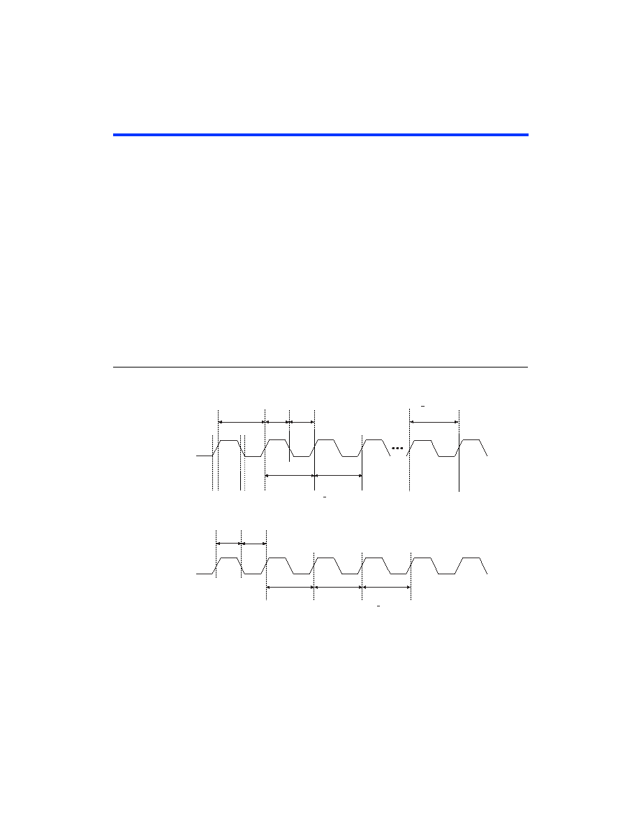
after configuration. Figure 19 shows the incoming and generated clock
specifications.
Figure 19. Specifications for the Incoming & Generated Clocks
Note:
(1)
The tI parameter refers to the nominal input clock period; the tO parameter refers to the nominal output clock
period.
Input
Clock
ClockLock
Generated
Clock
tCLK1
tINDUTY
tI+ tCLKDEV
tR
tF
tO
tI+ tINCLKSTB
tO
tO tJITTER
tO+ tJITTER
tOUTDUTY
相关PDF资料 |
PDF描述 |
|---|---|
| MAX6692MSA+ | IC SENSOR REMOTE SMBUS 8SOIC |
| RGF1M | DIODE GPP FAST 1A 1000V SMA |
| DSP56321VL200 | IC DSP 24BIT 200MHZ 196-MAPBGA |
| AGM30DRSN-S288 | CONN EDGECARD EXTEND 60POS .156 |
| IRS2168DPBF | IC PFC BALLAST CTLR ADV 16-PDIP |
相关代理商/技术参数 |
参数描述 |
|---|---|
| EP1K30FC256-3N | 功能描述:FPGA - 现场可编程门阵列 FPGA - ACEX 1K 216 LABs 171 IOs RoHS:否 制造商:Altera Corporation 系列:Cyclone V E 栅极数量: 逻辑块数量:943 内嵌式块RAM - EBR:1956 kbit 输入/输出端数量:128 最大工作频率:800 MHz 工作电源电压:1.1 V 最大工作温度:+ 70 C 安装风格:SMD/SMT 封装 / 箱体:FBGA-256 |
| EP1K30FI256-2 | 功能描述:FPGA - 现场可编程门阵列 FPGA - ACEX 1K 216 LABs 171 IOs RoHS:否 制造商:Altera Corporation 系列:Cyclone V E 栅极数量: 逻辑块数量:943 内嵌式块RAM - EBR:1956 kbit 输入/输出端数量:128 最大工作频率:800 MHz 工作电源电压:1.1 V 最大工作温度:+ 70 C 安装风格:SMD/SMT 封装 / 箱体:FBGA-256 |
| EP1K30FI256-2N | 功能描述:FPGA - 现场可编程门阵列 FPGA - ACEX 1K 216 LABs 171 IOs RoHS:否 制造商:Altera Corporation 系列:Cyclone V E 栅极数量: 逻辑块数量:943 内嵌式块RAM - EBR:1956 kbit 输入/输出端数量:128 最大工作频率:800 MHz 工作电源电压:1.1 V 最大工作温度:+ 70 C 安装风格:SMD/SMT 封装 / 箱体:FBGA-256 |
| EP1K30QC208-1 | 功能描述:FPGA - 现场可编程门阵列 FPGA - ACEX 1K 216 LABs 147 IOs RoHS:否 制造商:Altera Corporation 系列:Cyclone V E 栅极数量: 逻辑块数量:943 内嵌式块RAM - EBR:1956 kbit 输入/输出端数量:128 最大工作频率:800 MHz 工作电源电压:1.1 V 最大工作温度:+ 70 C 安装风格:SMD/SMT 封装 / 箱体:FBGA-256 |
| EP1K30QC208-1N | 功能描述:FPGA - 现场可编程门阵列 FPGA - ACEX 1K 216 LABs 147 IOs RoHS:否 制造商:Altera Corporation 系列:Cyclone V E 栅极数量: 逻辑块数量:943 内嵌式块RAM - EBR:1956 kbit 输入/输出端数量:128 最大工作频率:800 MHz 工作电源电压:1.1 V 最大工作温度:+ 70 C 安装风格:SMD/SMT 封装 / 箱体:FBGA-256 |
发布紧急采购,3分钟左右您将得到回复。