- 您现在的位置:买卖IC网 > PDF目录22034 > EP1K30TC144-3N (Altera)IC ACEX 1K FPGA 30K 144-TQFP PDF资料下载
参数资料
| 型号: | EP1K30TC144-3N |
| 厂商: | Altera |
| 文件页数: | 34/86页 |
| 文件大小: | 0K |
| 描述: | IC ACEX 1K FPGA 30K 144-TQFP |
| 产品培训模块: | Three Reasons to Use FPGA's in Industrial Designs |
| 标准包装: | 180 |
| 系列: | ACEX-1K® |
| LAB/CLB数: | 216 |
| 逻辑元件/单元数: | 1728 |
| RAM 位总计: | 24576 |
| 输入/输出数: | 102 |
| 门数: | 119000 |
| 电源电压: | 2.375 V ~ 2.625 V |
| 安装类型: | 表面贴装 |
| 工作温度: | 0°C ~ 85°C |
| 封装/外壳: | 144-LQFP |
| 供应商设备封装: | 144-TQFP(20x20) |
| 产品目录页面: | 602 (CN2011-ZH PDF) |
| 其它名称: | 544-1839 EP1K30TC144-3N-ND |
第1页第2页第3页第4页第5页第6页第7页第8页第9页第10页第11页第12页第13页第14页第15页第16页第17页第18页第19页第20页第21页第22页第23页第24页第25页第26页第27页第28页第29页第30页第31页第32页第33页当前第34页第35页第36页第37页第38页第39页第40页第41页第42页第43页第44页第45页第46页第47页第48页第49页第50页第51页第52页第53页第54页第55页第56页第57页第58页第59页第60页第61页第62页第63页第64页第65页第66页第67页第68页第69页第70页第71页第72页第73页第74页第75页第76页第77页第78页第79页第80页第81页第82页第83页第84页第85页第86页
4
Altera Corporation
ACEX 1K Programmable Logic Device Family Data Sheet
General
Description
Altera ACEX 1K devices provide a die-efficient, low-cost architecture by
combining look-up table (LUT) architecture with EABs. LUT-based logic
provides optimized performance and efficiency for data-path, register
intensive, mathematical, or digital signal processing (DSP) designs, while
EABs implement RAM, ROM, dual-port RAM, or first-in first-out (FIFO)
functions. These elements make ACEX 1K suitable for complex logic
functions and memory functions such as digital signal processing, wide
data-path manipulation, data transformation and microcontrollers, as
required in high-performance communications applications. Based on
reconfigurable CMOS SRAM elements, the ACEX 1K architecture
incorporates all features necessary to implement common gate array
megafunctions, along with a high pin count to enable an effective interface
with system components. The advanced process and the low voltage
requirement of the 2.5-V core allow ACEX 1K devices to meet the
requirements of low-cost, high-volume applications ranging from DSL
modems to low-cost switches.
The ability to reconfigure ACEX 1K devices enables complete testing prior
to shipment and allows the designer to focus on simulation and design
verification. ACEX 1K device reconfigurability eliminates inventory
management for gate array designs and test vector generation for fault
coverage.
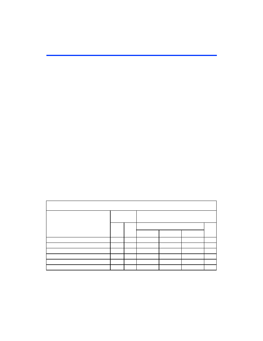
Table 4 shows ACEX 1K device performance for some common designs.
All performance results were obtained with Synopsys DesignWare or
LPM functions. Special design techniques are not required to implement
the applications; the designer simply infers or instantiates a function in a
Verilog HDL, VHDL, Altera Hardware Description Language (AHDL), or
schematic design file.
Notes:
(1)
This application uses combinatorial inputs and outputs.
(2)
This application uses registered inputs and outputs.
Table 4. ACEX 1K Device Performance
Application
Resources
Used
Performance
LEs
EABs
Speed Grade
Units
-1
-2
-3
16-bit loadable counter
16
0
285
232
185
MHz
16-bit accumulator
16
0
285
232
185
MHz
16-to-1 multiplexer (1)
10
0
3.5
4.5
6.6
ns
16-bit multiplier with 3-stage pipeline(2)
592
0
156
131
93
MHz
256
× 16 RAM read cycle speed (2)
0
1
278
196
143
MHz
256
× 16 RAM write cycle speed (2)
0
1
185
143
111
MHz
相关PDF资料 |
PDF描述 |
|---|---|
| 7-1624113-2 | INDUCTOR 2.7UH 5% 0805 |
| EP1K30TC144-3 | IC ACEX 1K FPGA 30K 144-TQFP |
| ADT7463ARQZ-REEL7 | IC REMOTE THERMAL CTRLR 24-QSOP |
| EPF6010ATC100-3N | IC FLEX 6000 FPGA 10K 100-TQFP |
| ADT7463ARQZ | IC REMOTE THERMAL CTRLR 24-QSOP |
相关代理商/技术参数 |
参数描述 |
|---|---|
| EP1K30TI144-2 | 功能描述:FPGA - 现场可编程门阵列 FPGA - ACEX 1K 216 LABs 102 IOs RoHS:否 制造商:Altera Corporation 系列:Cyclone V E 栅极数量: 逻辑块数量:943 内嵌式块RAM - EBR:1956 kbit 输入/输出端数量:128 最大工作频率:800 MHz 工作电源电压:1.1 V 最大工作温度:+ 70 C 安装风格:SMD/SMT 封装 / 箱体:FBGA-256 |
| EP1K30TI144-2N | 功能描述:FPGA - 现场可编程门阵列 FPGA - ACEX 1K 216 LABs 102 IOs RoHS:否 制造商:Altera Corporation 系列:Cyclone V E 栅极数量: 逻辑块数量:943 内嵌式块RAM - EBR:1956 kbit 输入/输出端数量:128 最大工作频率:800 MHz 工作电源电压:1.1 V 最大工作温度:+ 70 C 安装风格:SMD/SMT 封装 / 箱体:FBGA-256 |
| EP1K50 | 制造商:未知厂家 制造商全称:未知厂家 功能描述:Programmable Logic Device Family |
| EP1K50FC256-1 | 功能描述:FPGA - 现场可编程门阵列 FPGA - ACEX 1K 360 LABs 186 IOs RoHS:否 制造商:Altera Corporation 系列:Cyclone V E 栅极数量: 逻辑块数量:943 内嵌式块RAM - EBR:1956 kbit 输入/输出端数量:128 最大工作频率:800 MHz 工作电源电压:1.1 V 最大工作温度:+ 70 C 安装风格:SMD/SMT 封装 / 箱体:FBGA-256 |
| EP1K50FC256-1DX | 制造商:未知厂家 制造商全称:未知厂家 功能描述:Field Programmable Gate Array (FPGA) |
发布紧急采购,3分钟左右您将得到回复。