- 您现在的位置:买卖IC网 > PDF目录97912 > EP1K50FC484-3F Field Programmable Gate Array (FPGA) PDF资料下载
参数资料
| 型号: | EP1K50FC484-3F |
| 英文描述: | Field Programmable Gate Array (FPGA) |
| 中文描述: | 现场可编程门阵列(FPGA) |
| 文件页数: | 78/86页 |
| 文件大小: | 1263K |
| 代理商: | EP1K50FC484-3F |
第1页第2页第3页第4页第5页第6页第7页第8页第9页第10页第11页第12页第13页第14页第15页第16页第17页第18页第19页第20页第21页第22页第23页第24页第25页第26页第27页第28页第29页第30页第31页第32页第33页第34页第35页第36页第37页第38页第39页第40页第41页第42页第43页第44页第45页第46页第47页第48页第49页第50页第51页第52页第53页第54页第55页第56页第57页第58页第59页第60页第61页第62页第63页第64页第65页第66页第67页第68页第69页第70页第71页第72页第73页第74页第75页第76页第77页当前第78页第79页第80页第81页第82页第83页第84页第85页第86页
8
Altera Corporation
ACEX 1K Programmable Logic Device Family Data Sheet
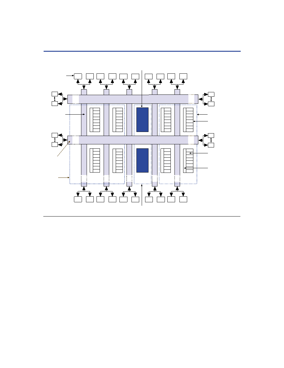
Figure 1. ACEX 1K Device Block Diagram
ACEX 1K devices provide six dedicated inputs that drive the flipflops’
control inputs and ensure the efficient distribution of high-speed, low-
skew (less than 1.0 ns) control signals. These signals use dedicated routing
channels that provide shorter delays and lower skews than the FastTrack
Interconnect routing structure. Four of the dedicated inputs drive four
global signals. These four global signals can also be driven by internal
logic, providing an ideal solution for a clock divider or an internally
generated asynchronous clear signal that clears many registers in the
device.
I/O Element
(IOE)
Logic Array
Block (LAB)
Row
Interconnect
IOE
Local Interconnect
IOE
Logic Element (LE)
Column
Interconnect
IOE
EAB
Logic
Array
IOE
Embedded Array Block (EAB)
Embedded Array
IOE
Logic Array
IOE
相关PDF资料 |
PDF描述 |
|---|---|
| EP1K50FI256-1DX | Field Programmable Gate Array (FPGA) |
| EP1K50FI256-1F | Dual LDO with Low Noise, Low IQ, and High PSRR; Temperature Range: -40°C to 85°C; Package: 10-DFN |
| EP1K50FI256-1P | Dual LDO with Low Noise, Low IQ, and High PSRR; Temperature Range: -40°C to 85°C; Package: 10-DFN |
| EP1K50FI256-1X | Field Programmable Gate Array (FPGA) |
| EP1K50FI256-2DX | Field Programmable Gate Array (FPGA) |
相关代理商/技术参数 |
参数描述 |
|---|---|
| EP1K50FC484-3N | 功能描述:FPGA - 现场可编程门阵列 FPGA - ACEX 1K 360 LABs 249 IOs RoHS:否 制造商:Altera Corporation 系列:Cyclone V E 栅极数量: 逻辑块数量:943 内嵌式块RAM - EBR:1956 kbit 输入/输出端数量:128 最大工作频率:800 MHz 工作电源电压:1.1 V 最大工作温度:+ 70 C 安装风格:SMD/SMT 封装 / 箱体:FBGA-256 |
| EP1K50FI256-1DX | 制造商:未知厂家 制造商全称:未知厂家 功能描述:Field Programmable Gate Array (FPGA) |
| EP1K50FI256-1F | 制造商:未知厂家 制造商全称:未知厂家 功能描述:Field Programmable Gate Array (FPGA) |
| EP1K50FI256-1P | 制造商:未知厂家 制造商全称:未知厂家 功能描述:Field Programmable Gate Array (FPGA) |
| EP1K50FI256-1X | 制造商:未知厂家 制造商全称:未知厂家 功能描述:Field Programmable Gate Array (FPGA) |
发布紧急采购,3分钟左右您将得到回复。