- 您现在的位置:买卖IC网 > PDF目录97925 > EP20K400GI655-3 RTC Module With CPU Supervisor PDF资料下载
参数资料
| 型号: | EP20K400GI655-3 |
| 元件分类: | CPU监测 |
| 英文描述: | RTC Module With CPU Supervisor |
| 中文描述: | 时钟模块CPU监控 |
| 文件页数: | 80/114页 |
| 文件大小: | 1623K |
| 代理商: | EP20K400GI655-3 |
第1页第2页第3页第4页第5页第6页第7页第8页第9页第10页第11页第12页第13页第14页第15页第16页第17页第18页第19页第20页第21页第22页第23页第24页第25页第26页第27页第28页第29页第30页第31页第32页第33页第34页第35页第36页第37页第38页第39页第40页第41页第42页第43页第44页第45页第46页第47页第48页第49页第50页第51页第52页第53页第54页第55页第56页第57页第58页第59页第60页第61页第62页第63页第64页第65页第66页第67页第68页第69页第70页第71页第72页第73页第74页第75页第76页第77页第78页第79页当前第80页第81页第82页第83页第84页第85页第86页第87页第88页第89页第90页第91页第92页第93页第94页第95页第96页第97页第98页第99页第100页第101页第102页第103页第104页第105页第106页第107页第108页第109页第110页第111页第112页第113页第114页
68
Altera Corporation
APEX 20K Programmable Logic Device Family Data Sheet
1
For DC Operating Specifications on APEX 20KE I/O standards,
please refer to Application Note 117 (Using Selectable I/O Standards
in Altera Devices).
Notes to tables:
(1)
See the Operating Requirements for Altera Devices Data Sheet.
(2)
Minimum DC input is –0.5 V. During transitions, the inputs may undershoot to –0.5 V or overshoot to 4.6 V for
input currents less than 100 mA and periods shorter than 20 ns.
(3)
Numbers in parentheses are for industrial-temperature-range devices.
(4)
Maximum VCC rise time is 100 ms, and VCC must rise monotonically.
(5)
All pins, including dedicated inputs, clock, I/O, and JTAG pins, may be driven before VCCINT and VCCIO are
powered.
(6)
Typical values are for TA = 25° C, VCCINT = 1.8 V, and VCCIO = 1.8V, 2.5V or 3.3V.
(7)
These values are specified under the APEX 20KE device recommended operating conditions, shown in Table 28 on
(8)
The APEX 20KE input buffers are compatible with 1.8-V, 2.5-V and 3.3-V (LVTTL and LVCMOS) signals.
Additionally, the input buffers are 3.3-V PCI compliant. Input buffers also meet specifications for GTL+, CTT, AGP,
SSTL-2, SSTL-3, and HSTL.
(9)
The IOH parameter refers to high-level TTL, PCI, or CMOS output current.
(10) The IOL parameter refers to low-level TTL, PCI, or CMOS output current. This parameter applies to open-drain pins
as well as output pins.
(11) This value is specified for normal device operation. The value may vary during power-up.
(12) Pin pull-up resistance values will be lower if an external source drives the pin higher than VCCIO.
(13) Capacitance is sample-tested only.
compliance on APEX 20K devices.
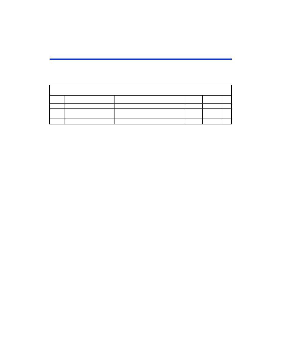
Table 34. APEX 20KE Device Capacitance
Symbol
Parameter
Conditions
Min
Max
Unit
CIN
Input capacitance
VIN = 0 V, f = 1.0 MHz
8
pF
CINCLK
Input capacitance on dedicated
clock pin
VIN = 0 V, f = 1.0 MHz
12
pF
COUT
Output capacitance
VOUT = 0 V, f = 1.0 MHz
8
pF
相关PDF资料 |
PDF描述 |
|---|---|
| EP20K400GI655-3ES | RTC Module With CPU Supervisor |
| EP20K600CB652I7ES | RTC Module With CPU Supervisor |
| EP20K600CB652I8ES | RTC Module With CPU Supervisor |
| EP20K600CB652I9ES | RTC Module With CPU Supervisor |
| EP20K600CF1020I7ES | RTC Module With CPU Supervisor |
相关代理商/技术参数 |
参数描述 |
|---|---|
| EP20K400GI655-3ES | 制造商:未知厂家 制造商全称:未知厂家 功能描述:FPGA |
| EP20K600C | 制造商:ALTERA 制造商全称:Altera Corporation 功能描述:Programmable Logic |
| EP20K600CB652C7 | 功能描述:FPGA - 现场可编程门阵列 CPLD - APEX 20K 2432 Macros 488 IO RoHS:否 制造商:Altera Corporation 系列:Cyclone V E 栅极数量: 逻辑块数量:943 内嵌式块RAM - EBR:1956 kbit 输入/输出端数量:128 最大工作频率:800 MHz 工作电源电压:1.1 V 最大工作温度:+ 70 C 安装风格:SMD/SMT 封装 / 箱体:FBGA-256 |
| EP20K600CB652C9 | 功能描述:FPGA - 现场可编程门阵列 CPLD - APEX 20K 2432 Macro 488 IOs RoHS:否 制造商:Altera Corporation 系列:Cyclone V E 栅极数量: 逻辑块数量:943 内嵌式块RAM - EBR:1956 kbit 输入/输出端数量:128 最大工作频率:800 MHz 工作电源电压:1.1 V 最大工作温度:+ 70 C 安装风格:SMD/SMT 封装 / 箱体:FBGA-256 |
| EP20K600CB652I7ES | 制造商:未知厂家 制造商全称:未知厂家 功能描述:ASIC |
发布紧急采购,3分钟左右您将得到回复。