- 您现在的位置:买卖IC网 > PDF目录19320 > EP2AGX125DF25C4N (Altera)IC ARRIA II GX FPGA 125K 572FBGA PDF资料下载
参数资料
| 型号: | EP2AGX125DF25C4N |
| 厂商: | Altera |
| 文件页数: | 21/90页 |
| 文件大小: | 0K |
| 描述: | IC ARRIA II GX FPGA 125K 572FBGA |
| 产品培训模块: | Three Reasons to Use FPGA's in Industrial Designs |
| 标准包装: | 5 |
| 系列: | Arria II GX |
| LAB/CLB数: | 4964 |
| 逻辑元件/单元数: | 118143 |
| RAM 位总计: | 8315904 |
| 输入/输出数: | 260 |
| 电源电压: | 0.87 V ~ 0.93 V |
| 安装类型: | 表面贴装 |
| 工作温度: | 0°C ~ 85°C |
| 封装/外壳: | 572-FBGA |
| 供应商设备封装: | 572-FBGA |
| 其它名称: | 544-2710 |
第1页第2页第3页第4页第5页第6页第7页第8页第9页第10页第11页第12页第13页第14页第15页第16页第17页第18页第19页第20页当前第21页第22页第23页第24页第25页第26页第27页第28页第29页第30页第31页第32页第33页第34页第35页第36页第37页第38页第39页第40页第41页第42页第43页第44页第45页第46页第47页第48页第49页第50页第51页第52页第53页第54页第55页第56页第57页第58页第59页第60页第61页第62页第63页第64页第65页第66页第67页第68页第69页第70页第71页第72页第73页第74页第75页第76页第77页第78页第79页第80页第81页第82页第83页第84页第85页第86页第87页第88页第89页第90页
1–20
Chapter 1: Device Datasheet for Arria II Devices
Electrical Characteristics
December 2013
Altera Corporation
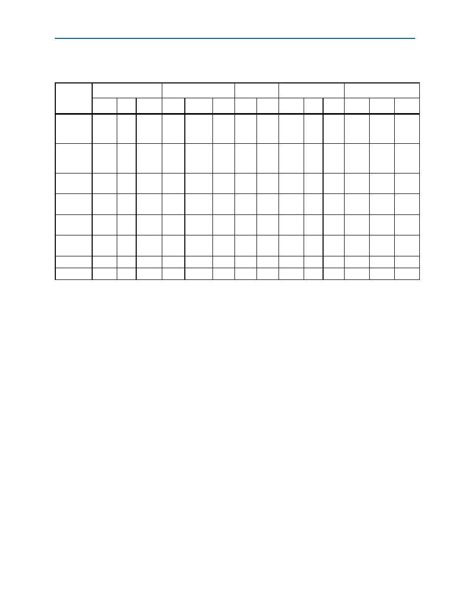
Table 1–33 lists the differential I/O standard specifications for Arria II GZ devices.
Power Consumption for the Arria II Device Family
Altera offers two ways to estimate power for a design:
■
Using the Microsoft Excel-based Early Power Estimator
■
Using the Quartus II PowerPlay Power Analyzer feature
The interactive Microsoft Excel-based Early Power Estimator is typically used prior to
designing the FPGA in order to get a magnitude estimate of the device power. The
Quartus II PowerPlay Power Analyzer provides better quality estimates based on the
specifics of the design after place-and-route is complete. The PowerPlay Power
Analyzer can apply a combination of user-entered, simulation-derived, and estimated
signal activities which, when combined with detailed circuit models, can yield very
accurate power estimates.
f For more information about power estimation tools, refer to the PowerPlay Early Power
Estimator User Guide and the PowerPlay Power Analysis chapter in volume 3 of the
Quartus II Handbook.
Table 1–33. Differential I/O Standard Specifications for Arria II GZ Devices (Note 1)
I/O
Standard
VCCIO (V)
VID (mV)
VICM(DC) (V)
Min
Typ
Max
Min
Cond.
Max
Min
Max
Min
Typ
Max
Min
Typ
Max
2.5 V
LVDS
(HIO)
2.375
2.5
2.625
100
VCM =
1.25 V
—
0.05
1.8
0.247
—
0.6
1.125
1.25
1.375
2.5 V
LVDS
(VIO)
2.375
2.5
2.625
100
VCM =
1.25 V
—
0.05
1.8
0.247
—
0.6
1
1.25
1.5
RSDS
(HIO)
2.375
2.5
2.625
100
VCM =
1.25 V
—
0.3
1.4
0.1
0.2
0.6
0.5
1.2
1.4
RSDS
(VIO)
2.375
2.5
2.625
100
VCM =
1.25 V
—
0.3
1.4
0.1
0.2
0.6
0.5
1.2
1.5
Mini-LVDS
(HIO)
2.375
2.5
2.625
200
—
600
0.4
1.32
5
0.25
—
0.6
1
1.2
1.4
Mini-LVDS
(VIO)
2.375
2.5
2.625
200
—
600
0.4
1.32
5
0.25
—
0.6
1
1.2
1.5
LVPECL
2.375
2.5
2.625
300
—
0.6
1.8
—
BLVDS (4)
2.375
2.5
2.625
100
—
Notes to Table 1–33:
(1) 1.4-V/1.5-V PCML transceiver I/O standard specifications are described in “Transceiver Performance Specifications” on page 1–21.
(2) Vertical I/O (VIO) is top and bottom I/Os; horizontal I/O (HIO) is left and right I/Os.
(3) RL range: 90 RL 110 .
(4) There are no fixed VICM, VOD, and VOCM specifications for BLVDS. These specifications depend on the system topology.
相关PDF资料 |
PDF描述 |
|---|---|
| ECM10DRTI-S13 | CONN EDGECARD 20POS .156 EXTEND |
| VI-B6B-EU-S | CONVERTER MOD DC/DC 95V 200W |
| SS24T3G | DIODE SCHOTTKY POWER 2A 40V SMB |
| EP1S30F780C6N | IC STRATIX FPGA 30K LE 780-FBGA |
| MCP9802A5T-M/OTG | IC SENSOR THERMAL 2.7V SOT23-5 |
相关代理商/技术参数 |
参数描述 |
|---|---|
| EP2AGX125DF25C5 | 功能描述:FPGA - 现场可编程门阵列 FPGA - Arria II GX 4964 LABs 260 IOs RoHS:否 制造商:Altera Corporation 系列:Cyclone V E 栅极数量: 逻辑块数量:943 内嵌式块RAM - EBR:1956 kbit 输入/输出端数量:128 最大工作频率:800 MHz 工作电源电压:1.1 V 最大工作温度:+ 70 C 安装风格:SMD/SMT 封装 / 箱体:FBGA-256 |
| EP2AGX125DF25C5N | 功能描述:FPGA - 现场可编程门阵列 FPGA - Arria II GX 4964 LABs 260 IOs RoHS:否 制造商:Altera Corporation 系列:Cyclone V E 栅极数量: 逻辑块数量:943 内嵌式块RAM - EBR:1956 kbit 输入/输出端数量:128 最大工作频率:800 MHz 工作电源电压:1.1 V 最大工作温度:+ 70 C 安装风格:SMD/SMT 封装 / 箱体:FBGA-256 |
| EP2AGX125DF25C5NES | 制造商:Altera Corporation 功能描述:IC ARRIA II GX FPGA 572FBGA 制造商:Altera Corporation 功能描述:IC FPGA 260 I/O 572FBGA |
| EP2AGX125DF25C6 | 功能描述:FPGA - 现场可编程门阵列 FPGA - Arria II GX 4964 LABs 260 IOs RoHS:否 制造商:Altera Corporation 系列:Cyclone V E 栅极数量: 逻辑块数量:943 内嵌式块RAM - EBR:1956 kbit 输入/输出端数量:128 最大工作频率:800 MHz 工作电源电压:1.1 V 最大工作温度:+ 70 C 安装风格:SMD/SMT 封装 / 箱体:FBGA-256 |
| EP2AGX125DF25C6N | 功能描述:FPGA - 现场可编程门阵列 FPGA - Arria II GX 4964 LABs 260 IOs RoHS:否 制造商:Altera Corporation 系列:Cyclone V E 栅极数量: 逻辑块数量:943 内嵌式块RAM - EBR:1956 kbit 输入/输出端数量:128 最大工作频率:800 MHz 工作电源电压:1.1 V 最大工作温度:+ 70 C 安装风格:SMD/SMT 封装 / 箱体:FBGA-256 |
发布紧急采购,3分钟左右您将得到回复。