参数资料
| 型号: | EP2AGX260FF35C4 |
| 厂商: | Altera |
| 文件页数: | 84/90页 |
| 文件大小: | 0K |
| 描述: | IC ARRIA II GX 260K 1152FBGA |
| 产品培训模块: | Three Reasons to Use FPGA's in Industrial Designs |
| 标准包装: | 3 |
| 系列: | Arria II GX |
| LAB/CLB数: | 10260 |
| 逻辑元件/单元数: | 244188 |
| RAM 位总计: | 12038144 |
| 输入/输出数: | 612 |
| 电源电压: | 0.87 V ~ 0.93 V |
| 安装类型: | 表面贴装 |
| 工作温度: | 0°C ~ 85°C |
| 封装/外壳: | 1152-BBGA |
| 供应商设备封装: | 1152-FBGA(27x27) |
第1页第2页第3页第4页第5页第6页第7页第8页第9页第10页第11页第12页第13页第14页第15页第16页第17页第18页第19页第20页第21页第22页第23页第24页第25页第26页第27页第28页第29页第30页第31页第32页第33页第34页第35页第36页第37页第38页第39页第40页第41页第42页第43页第44页第45页第46页第47页第48页第49页第50页第51页第52页第53页第54页第55页第56页第57页第58页第59页第60页第61页第62页第63页第64页第65页第66页第67页第68页第69页第70页第71页第72页第73页第74页第75页第76页第77页第78页第79页第80页第81页第82页第83页当前第84页第85页第86页第87页第88页第89页第90页
Chapter 1: Device Datasheet for Arria II Devices
1–77
Document Revision History
December 2013
Altera Corporation
Document Revision History
Table 1–69 lists the revision history for this chapter.
U,
V
VCM(DC)
DC common mode input voltage.
VICM
Input common mode voltage: The common mode of the differential signal at the receiver.
VID
Input differential voltage swing: The difference in voltage between the positive and
complementary conductors of a differential transmission at the receiver.
VDIF(AC)
AC differential input voltage: Minimum AC input differential voltage required for switching.
VDIF(DC)
DC differential input voltage: Minimum DC input differential voltage required for switching.
VIH
Voltage input high: The minimum positive voltage applied to the input which is accepted by the
device as a logic high.
VIH(AC)
High-level AC input voltage.
VIH(DC)
High-level DC input voltage.
VIL
Voltage input low: The maximum positive voltage applied to the input which is accepted by the
device as a logic low.
VIL(AC)
Low-level AC input voltage.
VIL(DC)
Low-level DC input voltage.
VOCM
Output common mode voltage: The common mode of the differential signal at the transmitter.
VOD
Output differential voltage swing: The difference in voltage between the positive and
complementary conductors of a differential transmission at the transmitter.
W,
X,
Y,
Z
W
High-speed I/O block: The clock boost factor.
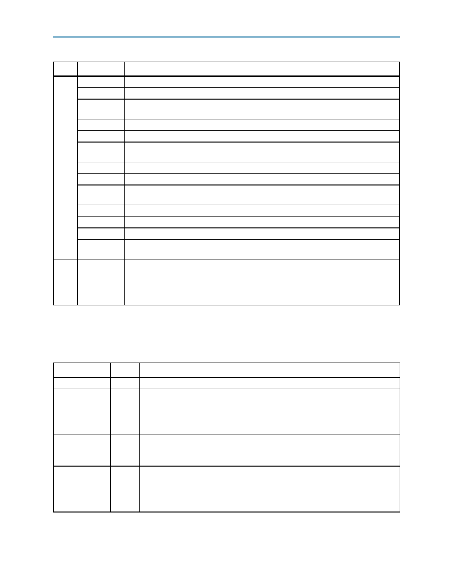
Table 1–68. Glossary (Part 4 of 4)
Letter
Subject
Definitions
Table 1–69. Document Revision History (Part 1 of 2)
Date
Version
Changes
December 2013
4.4
Updated Table 1–34 and Table 1–35.
July 2012
4.3
■ Updated the VCCH_GXBL/R operating conditions in Table 1–6.
■ Finalized Arria II GZ information in Table 1–20.
■ Added BLVDS specification in Table 1–32 and Table 1–33.
■ Updated input and output waveforms in Table 1–68.
December 2011
4.2
■ Updated Table 1–32, Table 1–33, Table 1–34, Table 1–35, Table 1–40, Table 1–41,
Table 1–54, and Table 1–67.
■ Minor text edits.
June 2011
4.1
■ Added Table 1–60.
■ Updated Table 1–32, Table 1–33, Table 1–38, Table 1–41, and Table 1–61.
■ Updated the “Switching Characteristics” section introduction.
■ Minor text edits.
相关PDF资料 |
PDF描述 |
|---|---|
| EP4SGX110HF35I4N | IC STRATIX IV FPGA 110K 1152FBGA |
| EP4SGX110HF35C3N | IC STRATIX IV FPGA 110K 1152FBGA |
| A54SX16-1CQ256B | IC FPGA SX 24K GATES 256-CQFP |
| EP4SGX180FF35C4N | IC STRATIX IV FPGA 180K 1152FBGA |
| A54SX32A-CQ84B | IC FPGA SX 48K GATES 84-CQFP |
相关代理商/技术参数 |
参数描述 |
|---|---|
| EP2AGX260FF35C4N | 功能描述:FPGA - 现场可编程门阵列 FPGA - Arria II GX 10260 LABs 612 IO RoHS:否 制造商:Altera Corporation 系列:Cyclone V E 栅极数量: 逻辑块数量:943 内嵌式块RAM - EBR:1956 kbit 输入/输出端数量:128 最大工作频率:800 MHz 工作电源电压:1.1 V 最大工作温度:+ 70 C 安装风格:SMD/SMT 封装 / 箱体:FBGA-256 |
| EP2AGX260FF35C5 | 功能描述:FPGA - 现场可编程门阵列 FPGA - Arria II GX 10260 LABs 612 IO RoHS:否 制造商:Altera Corporation 系列:Cyclone V E 栅极数量: 逻辑块数量:943 内嵌式块RAM - EBR:1956 kbit 输入/输出端数量:128 最大工作频率:800 MHz 工作电源电压:1.1 V 最大工作温度:+ 70 C 安装风格:SMD/SMT 封装 / 箱体:FBGA-256 |
| EP2AGX260FF35C5N | 功能描述:FPGA - 现场可编程门阵列 FPGA - Arria II GX 10260 LABs 612 IO RoHS:否 制造商:Altera Corporation 系列:Cyclone V E 栅极数量: 逻辑块数量:943 内嵌式块RAM - EBR:1956 kbit 输入/输出端数量:128 最大工作频率:800 MHz 工作电源电压:1.1 V 最大工作温度:+ 70 C 安装风格:SMD/SMT 封装 / 箱体:FBGA-256 |
| EP2AGX260FF35C6 | 功能描述:FPGA - 现场可编程门阵列 FPGA - Arria II GX 10260 LABs 612 IO RoHS:否 制造商:Altera Corporation 系列:Cyclone V E 栅极数量: 逻辑块数量:943 内嵌式块RAM - EBR:1956 kbit 输入/输出端数量:128 最大工作频率:800 MHz 工作电源电压:1.1 V 最大工作温度:+ 70 C 安装风格:SMD/SMT 封装 / 箱体:FBGA-256 |
| EP2AGX260FF35C6N | 功能描述:FPGA - 现场可编程门阵列 FPGA - Arria II GX 10260 LABs 612 IO RoHS:否 制造商:Altera Corporation 系列:Cyclone V E 栅极数量: 逻辑块数量:943 内嵌式块RAM - EBR:1956 kbit 输入/输出端数量:128 最大工作频率:800 MHz 工作电源电压:1.1 V 最大工作温度:+ 70 C 安装风格:SMD/SMT 封装 / 箱体:FBGA-256 |
发布紧急采购,3分钟左右您将得到回复。