参数资料
| 型号: | EP4CE10F17I7 |
| 厂商: | Altera |
| 文件页数: | 28/42页 |
| 文件大小: | 0K |
| 描述: | IC CYCLONE IV FPGA 10K 256FBGA |
| 产品培训模块: | Three Reasons to Use FPGA's in Industrial Designs Cyclone IV FPGA Family Overview |
| 特色产品: | Cyclone? IV FPGAs |
| 标准包装: | 90 |
| 系列: | CYCLONE® IV E |
| LAB/CLB数: | 645 |
| 逻辑元件/单元数: | 10320 |
| RAM 位总计: | 423936 |
| 输入/输出数: | 179 |
| 电源电压: | 1.15 V ~ 1.25 V |
| 安装类型: | 表面贴装 |
| 工作温度: | -40°C ~ 100°C |
| 封装/外壳: | 256-BGA |
| 供应商设备封装: | 256-FBGA(17x17) |
第1页第2页第3页第4页第5页第6页第7页第8页第9页第10页第11页第12页第13页第14页第15页第16页第17页第18页第19页第20页第21页第22页第23页第24页第25页第26页第27页当前第28页第29页第30页第31页第32页第33页第34页第35页第36页第37页第38页第39页第40页第41页第42页
1–34
Chapter 1: Cyclone IV Device Datasheet
Switching Characteristics
December 2013
Altera Corporation
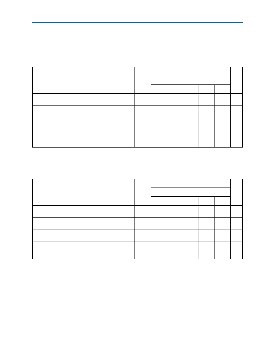
IOE Programmable Delay
Table 1–40 and Table 1–41 list the IOE programmable delay for Cyclone IV E 1.0 V
core voltage devices.
Table 1–40. IOE Programmable Delay on Column Pins for Cyclone IV E 1.0 V Core Voltage Devices (1), (2)
Parameter
Paths Affected
Number
of
Setting
Min
Offset
Max Offset
Unit
Fast Corner
Slow Corner
C8L
I8L
C8L
C9L
I8L
Input delay from pin to
internal cells
Pad to I/O
dataout to core
7
0
2.054
1.924
3.387
4.017
3.411
ns
Input delay from pin to
input register
Pad to I/O input
register
8
0
2.010
1.875
3.341
4.252
3.367
ns
Delay from output register
to output pin
I/O output
register to pad
2
0
0.641
0.631
1.111
1.377
1.124
ns
Input delay from
dual-purpose clock pin to
fan-out destinations
Pad to global
clock network
12
0
0.971
0.931
1.684
2.298
1.684
ns
Notes to Table 1–40:
(1) The incremental values for the settings are generally linear. For the exact values for each setting, use the latest version of the Quartus II software.
(2) The minimum and maximum offset timing numbers are in reference to setting 0 as available in the Quartus II software.
Table 1–41. IOE Programmable Delay on Row Pins for Cyclone IV E 1.0 V Core Voltage Devices (1), (2)
Parameter
Paths Affected
Number
of
Setting
Min
Offset
Max Offset
Unit
Fast Corner
Slow Corner
C8L
I8L
C8L
C9L
I8L
Input delay from pin to
internal cells
Pad to I/O
dataout to core
7
0
2.057
1.921
3.389
4.146
3.412
ns
Input delay from pin to
input register
Pad to I/O input
register
8
0
2.059
1.919
3.420
4.374
3.441
ns
Delay from output register
to output pin
I/O output
register to pad
2
0
0.670
0.623
1.160
1.420
1.168
ns
Input delay from
dual-purpose clock pin to
fan-out destinations
Pad to global
clock network
12
0
0.960
0.919
1.656
2.258
1.656
ns
Notes to Table 1–41:
(1) The incremental values for the settings are generally linear. For the exact values for each setting, use the latest version of the Quartus II software.
(2) The minimum and maximum offset timing numbers are in reference to setting 0 as available in the Quartus II software.
相关PDF资料 |
PDF描述 |
|---|---|
| EP4CE10F17C6 | IC CYCLONE IV FPGA 10K 256FBGA |
| EP4CE22E22C8LN | IC CYCLONE IV FPGA 22K 144EQFP |
| EP4CE22F17C9LN | IC CYCLONE IV FPGA 22K 256FBGA |
| M1A3P400-2PQG208 | IC FPGA 1KB FLASH 400K 208-PQFP |
| A3P400-2PQG208 | IC FPGA 1KB FLASH 400K 208-PQFP |
相关代理商/技术参数 |
参数描述 |
|---|---|
| EP4CE10F17I7N | 功能描述:FPGA - 现场可编程门阵列 FPGA - Cyclone IV E 645 LABs 179 IOs RoHS:否 制造商:Altera Corporation 系列:Cyclone V E 栅极数量: 逻辑块数量:943 内嵌式块RAM - EBR:1956 kbit 输入/输出端数量:128 最大工作频率:800 MHz 工作电源电压:1.1 V 最大工作温度:+ 70 C 安装风格:SMD/SMT 封装 / 箱体:FBGA-256 |
| EP4CE10F17I8L | 功能描述:FPGA - 现场可编程门阵列 FPGA - Cyclone IV E 645 LABs 179 IOs RoHS:否 制造商:Altera Corporation 系列:Cyclone V E 栅极数量: 逻辑块数量:943 内嵌式块RAM - EBR:1956 kbit 输入/输出端数量:128 最大工作频率:800 MHz 工作电源电压:1.1 V 最大工作温度:+ 70 C 安装风格:SMD/SMT 封装 / 箱体:FBGA-256 |
| EP4CE10F17I8LN | 功能描述:FPGA - 现场可编程门阵列 FPGA - Cyclone IV E 645 LABs 179 IOs RoHS:否 制造商:Altera Corporation 系列:Cyclone V E 栅极数量: 逻辑块数量:943 内嵌式块RAM - EBR:1956 kbit 输入/输出端数量:128 最大工作频率:800 MHz 工作电源电压:1.1 V 最大工作温度:+ 70 C 安装风格:SMD/SMT 封装 / 箱体:FBGA-256 |
| EP4CE10F23C8N | 制造商:ALTERA 制造商全称:Altera Corporation 功能描述:Cyclone IV FPGA Device Faily Overview |
| EP4CE10F23I7N | 制造商:ALTERA 制造商全称:Altera Corporation 功能描述:Cyclone IV Device Datasheet |
发布紧急采购,3分钟左右您将得到回复。