参数资料
| 型号: | EP4CE75F29C8 |
| 厂商: | Altera |
| 文件页数: | 16/42页 |
| 文件大小: | 0K |
| 描述: | IC CYCLONE IV FPGA 75K 780FBGA |
| 产品培训模块: | Three Reasons to Use FPGA's in Industrial Designs Cyclone IV FPGA Family Overview |
| 特色产品: | Cyclone? IV FPGAs |
| 标准包装: | 36 |
| 系列: | CYCLONE® IV E |
| LAB/CLB数: | 4713 |
| 逻辑元件/单元数: | 75408 |
| RAM 位总计: | 2810880 |
| 输入/输出数: | 426 |
| 电源电压: | 1.15 V ~ 1.25 V |
| 安装类型: | 表面贴装 |
| 工作温度: | 0°C ~ 85°C |
| 封装/外壳: | 780-BBGA |
| 供应商设备封装: | 780-FBGA(29x29) |
第1页第2页第3页第4页第5页第6页第7页第8页第9页第10页第11页第12页第13页第14页第15页当前第16页第17页第18页第19页第20页第21页第22页第23页第24页第25页第26页第27页第28页第29页第30页第31页第32页第33页第34页第35页第36页第37页第38页第39页第40页第41页第42页
Chapter 1: Cyclone IV Device Datasheet
1–23
Switching Characteristics
December 2013
Altera Corporation
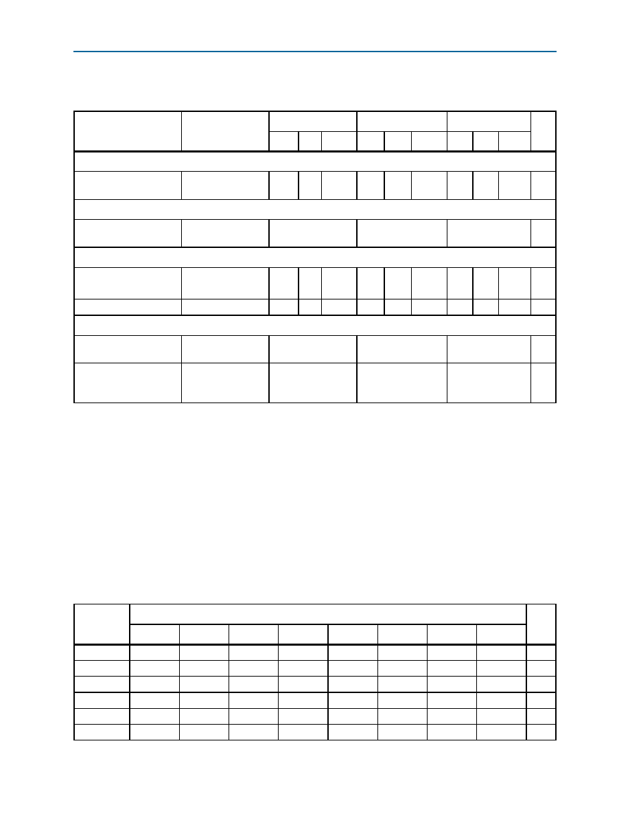
Table 1–23 lists the Cyclone IV GX transceiver block AC specifications.
Core Performance Specifications
The following sections describe the clock tree specifications, PLLs, embedded
multiplier, memory block, and configuration specifications for Cyclone IV Devices.
Clock Tree Specifications
Table 1–24 lists the clock tree specifications for Cyclone IV devices.
Table 1–23. Transceiver Block AC Specification for Cyclone IV GX Devices (1), (2)
Symbol/
Description
Conditions
C6
C7, I7
C8
Unit
Min
Typ
Max
Min
Typ
Max
Min
Typ
Max
PCIe Transmit Jitter Generation (3)
Total jitter at 2.5 Gbps
(Gen1)
Compliance pattern
—
0.25
—
0.25
—
0.25
UI
PCIe Receiver Jitter Tolerance (3)
Total jitter at 2.5 Gbps
(Gen1)
Compliance pattern
> 0.6
UI
GIGE Transmit Jitter Generation (4)
Deterministic jitter
(peak-to-peak)
Pattern = CRPAT
—
0.14—
—0.14
—
0.14
UI
Total jitter (peak-to-peak)
Pattern = CRPAT
—
0.279
—
0.279
—
0.279
UI
GIGE Receiver Jitter Tolerance (4)
Deterministic jitter
tolerance (peak-to-peak)
Pattern = CJPAT
> 0.4
UI
Combined deterministic
and random jitter
tolerance (peak-to-peak)
Pattern = CJPAT
> 0.66
UI
Notes to Table 1–23:
(1) Dedicated refclk pins were used to drive the input reference clocks.
(2) The jitter numbers specified are valid for the stated conditions only.
(3) The jitter numbers for PIPE are compliant to the PCIe Base Specification 2.0.
(4) The jitter numbers for GIGE are compliant to the IEEE802.3-2002 Specification.
Table 1–24. Clock Tree Performance for Cyclone IV Devices (Part 1 of 2)
Device
Performance
Unit
C6
C7
C8
C8L (1)
C9L (1)
I7
I8L (1)
A7
EP4CE6
500
437.5
402
362
265
437.5
362
402
MHz
EP4CE10
500
437.5
402
362
265
437.5
362
402
MHz
EP4CE15
500
437.5
402
362
265
437.5
362
402
MHz
EP4CE22
500
437.5
402
362
265
437.5
362
402
MHz
EP4CE30
500
437.5
402
362
265
437.5
362
402
MHz
EP4CE40
500
437.5
402
362
265
437.5
362
402
MHz
相关PDF资料 |
PDF描述 |
|---|---|
| M1AGL1000V2-FGG256I | IC FPGA 1KB FLASH 1M 256-FBGA |
| AGL1000V2-FG256I | IC FPGA 1KB FLASH 1M 256FBGA |
| AGL1000V2-FGG256I | IC FPGA 1KB FLASH 1M 256FBGA |
| M1AGL1000V2-FG256I | IC FPGA 1KB FLASH 1M 256-FBGA |
| A42MX24-3PQ160 | IC FPGA MX SGL CHIP 36K 160-PQFP |
相关代理商/技术参数 |
参数描述 |
|---|---|
| EP4CE75F29C8L | 功能描述:FPGA - 现场可编程门阵列 FPGA - Cyclone IV E 4713 LABs 426 IOs RoHS:否 制造商:Altera Corporation 系列:Cyclone V E 栅极数量: 逻辑块数量:943 内嵌式块RAM - EBR:1956 kbit 输入/输出端数量:128 最大工作频率:800 MHz 工作电源电压:1.1 V 最大工作温度:+ 70 C 安装风格:SMD/SMT 封装 / 箱体:FBGA-256 |
| EP4CE75F29C8LN | 功能描述:FPGA - 现场可编程门阵列 FPGA - Cyclone IV E 4713 LABs 426 IOs RoHS:否 制造商:Altera Corporation 系列:Cyclone V E 栅极数量: 逻辑块数量:943 内嵌式块RAM - EBR:1956 kbit 输入/输出端数量:128 最大工作频率:800 MHz 工作电源电压:1.1 V 最大工作温度:+ 70 C 安装风格:SMD/SMT 封装 / 箱体:FBGA-256 |
| EP4CE75F29C8N | 功能描述:FPGA - 现场可编程门阵列 FPGA - Cyclone IV E 4713 LABs 426 IOs RoHS:否 制造商:Altera Corporation 系列:Cyclone V E 栅极数量: 逻辑块数量:943 内嵌式块RAM - EBR:1956 kbit 输入/输出端数量:128 最大工作频率:800 MHz 工作电源电压:1.1 V 最大工作温度:+ 70 C 安装风格:SMD/SMT 封装 / 箱体:FBGA-256 |
| EP4CE75F29C9L | 功能描述:FPGA - 现场可编程门阵列 FPGA - Cyclone IV E 4713 LABs 426 IOs RoHS:否 制造商:Altera Corporation 系列:Cyclone V E 栅极数量: 逻辑块数量:943 内嵌式块RAM - EBR:1956 kbit 输入/输出端数量:128 最大工作频率:800 MHz 工作电源电压:1.1 V 最大工作温度:+ 70 C 安装风格:SMD/SMT 封装 / 箱体:FBGA-256 |
| EP4CE75F29C9LN | 功能描述:FPGA - 现场可编程门阵列 FPGA - Cyclone IV E 4713 LABs 426 IOs RoHS:否 制造商:Altera Corporation 系列:Cyclone V E 栅极数量: 逻辑块数量:943 内嵌式块RAM - EBR:1956 kbit 输入/输出端数量:128 最大工作频率:800 MHz 工作电源电压:1.1 V 最大工作温度:+ 70 C 安装风格:SMD/SMT 封装 / 箱体:FBGA-256 |
发布紧急采购,3分钟左右您将得到回复。