参数资料
| 型号: | EP4CE75F29C8 |
| 厂商: | Altera |
| 文件页数: | 35/42页 |
| 文件大小: | 0K |
| 描述: | IC CYCLONE IV FPGA 75K 780FBGA |
| 产品培训模块: | Three Reasons to Use FPGA's in Industrial Designs Cyclone IV FPGA Family Overview |
| 特色产品: | Cyclone? IV FPGAs |
| 标准包装: | 36 |
| 系列: | CYCLONE® IV E |
| LAB/CLB数: | 4713 |
| 逻辑元件/单元数: | 75408 |
| RAM 位总计: | 2810880 |
| 输入/输出数: | 426 |
| 电源电压: | 1.15 V ~ 1.25 V |
| 安装类型: | 表面贴装 |
| 工作温度: | 0°C ~ 85°C |
| 封装/外壳: | 780-BBGA |
| 供应商设备封装: | 780-FBGA(29x29) |
第1页第2页第3页第4页第5页第6页第7页第8页第9页第10页第11页第12页第13页第14页第15页第16页第17页第18页第19页第20页第21页第22页第23页第24页第25页第26页第27页第28页第29页第30页第31页第32页第33页第34页当前第35页第36页第37页第38页第39页第40页第41页第42页
1–40
Chapter 1: Cyclone IV Device Datasheet
Glossary
December 2013
Altera Corporation
T
tC
High-speed receiver and transmitter input and output clock period.
Channel-to-
channel-skew
(TCCS)
High-speed I/O block: The timing difference between the fastest and slowest output edges,
including tCO variation and clock skew. The clock is included in the TCCS measurement.
tcin
Delay from the clock pad to the I/O input register.
tCO
Delay from the clock pad to the I/O output.
tcout
Delay from the clock pad to the I/O output register.
tDUTY
High-speed I/O block: Duty cycle on high-speed transmitter output clock.
tFALL
Signal high-to-low transition time (80–20%).
tH
Input register hold time.
Timing Unit
Interval (TUI)
High-speed I/O block: The timing budget allowed for skew, propagation delays, and data
sampling window. (TUI = 1/(Receiver Input Clock Frequency Multiplication Factor) = tC/w).
tINJITTER
Period jitter on the PLL clock input.
tOUTJITTER_DEDCLK
Period jitter on the dedicated clock output driven by a PLL.
tOUTJITTER_IO
Period jitter on the general purpose I/O driven by a PLL.
tpllcin
Delay from the PLL inclk pad to the I/O input register.
tpllcout
Delay from the PLL inclk pad to the I/O output register.
Transmitter
Output
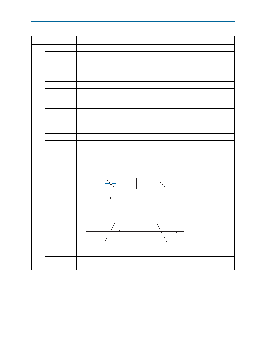
Waveform
Transmitter output waveforms for the LVDS, mini-LVDS, PPDS and RSDS Differential I/O
Standards:
tRISE
Signal low-to-high transition time (20–80%).
tSU
Input register setup time.
U
——
Table 1–46. Glossary (Part 4 of 5)
Letter
Term
Definitions
Single-Ended Waveform
Differential Waveform (Mathematical Function of Positive & Negative Channel)
Positive Channel (p) = V
OH
Negative Channel (n) = V
OL
Ground
VOD
V
OD
V
OD
0 V
Vos
p
- n
相关PDF资料 |
PDF描述 |
|---|---|
| M1AGL1000V2-FGG256I | IC FPGA 1KB FLASH 1M 256-FBGA |
| AGL1000V2-FG256I | IC FPGA 1KB FLASH 1M 256FBGA |
| AGL1000V2-FGG256I | IC FPGA 1KB FLASH 1M 256FBGA |
| M1AGL1000V2-FG256I | IC FPGA 1KB FLASH 1M 256-FBGA |
| A42MX24-3PQ160 | IC FPGA MX SGL CHIP 36K 160-PQFP |
相关代理商/技术参数 |
参数描述 |
|---|---|
| EP4CE75F29C8L | 功能描述:FPGA - 现场可编程门阵列 FPGA - Cyclone IV E 4713 LABs 426 IOs RoHS:否 制造商:Altera Corporation 系列:Cyclone V E 栅极数量: 逻辑块数量:943 内嵌式块RAM - EBR:1956 kbit 输入/输出端数量:128 最大工作频率:800 MHz 工作电源电压:1.1 V 最大工作温度:+ 70 C 安装风格:SMD/SMT 封装 / 箱体:FBGA-256 |
| EP4CE75F29C8LN | 功能描述:FPGA - 现场可编程门阵列 FPGA - Cyclone IV E 4713 LABs 426 IOs RoHS:否 制造商:Altera Corporation 系列:Cyclone V E 栅极数量: 逻辑块数量:943 内嵌式块RAM - EBR:1956 kbit 输入/输出端数量:128 最大工作频率:800 MHz 工作电源电压:1.1 V 最大工作温度:+ 70 C 安装风格:SMD/SMT 封装 / 箱体:FBGA-256 |
| EP4CE75F29C8N | 功能描述:FPGA - 现场可编程门阵列 FPGA - Cyclone IV E 4713 LABs 426 IOs RoHS:否 制造商:Altera Corporation 系列:Cyclone V E 栅极数量: 逻辑块数量:943 内嵌式块RAM - EBR:1956 kbit 输入/输出端数量:128 最大工作频率:800 MHz 工作电源电压:1.1 V 最大工作温度:+ 70 C 安装风格:SMD/SMT 封装 / 箱体:FBGA-256 |
| EP4CE75F29C9L | 功能描述:FPGA - 现场可编程门阵列 FPGA - Cyclone IV E 4713 LABs 426 IOs RoHS:否 制造商:Altera Corporation 系列:Cyclone V E 栅极数量: 逻辑块数量:943 内嵌式块RAM - EBR:1956 kbit 输入/输出端数量:128 最大工作频率:800 MHz 工作电源电压:1.1 V 最大工作温度:+ 70 C 安装风格:SMD/SMT 封装 / 箱体:FBGA-256 |
| EP4CE75F29C9LN | 功能描述:FPGA - 现场可编程门阵列 FPGA - Cyclone IV E 4713 LABs 426 IOs RoHS:否 制造商:Altera Corporation 系列:Cyclone V E 栅极数量: 逻辑块数量:943 内嵌式块RAM - EBR:1956 kbit 输入/输出端数量:128 最大工作频率:800 MHz 工作电源电压:1.1 V 最大工作温度:+ 70 C 安装风格:SMD/SMT 封装 / 箱体:FBGA-256 |
发布紧急采购,3分钟左右您将得到回复。