- 您现在的位置:买卖IC网 > PDF目录295888 > EPM2210GF256A4N (ALTERA CORP) FLASH PLD, PBGA256 PDF资料下载
参数资料
| 型号: | EPM2210GF256A4N |
| 厂商: | ALTERA CORP |
| 元件分类: | PLD |
| 英文描述: | FLASH PLD, PBGA256 |
| 封装: | 17 X 17 MM, 1 MM PITCH, LEAD FREE, FBGA-256 |
| 文件页数: | 62/108页 |
| 文件大小: | 1342K |
| 代理商: | EPM2210GF256A4N |
第1页第2页第3页第4页第5页第6页第7页第8页第9页第10页第11页第12页第13页第14页第15页第16页第17页第18页第19页第20页第21页第22页第23页第24页第25页第26页第27页第28页第29页第30页第31页第32页第33页第34页第35页第36页第37页第38页第39页第40页第41页第42页第43页第44页第45页第46页第47页第48页第49页第50页第51页第52页第53页第54页第55页第56页第57页第58页第59页第60页第61页当前第62页第63页第64页第65页第66页第67页第68页第69页第70页第71页第72页第73页第74页第75页第76页第77页第78页第79页第80页第81页第82页第83页第84页第85页第86页第87页第88页第89页第90页第91页第92页第93页第94页第95页第96页第97页第98页第99页第100页第101页第102页第103页第104页第105页第106页第107页第108页
Altera Corporation
Core Version a.b.c variable
3–7
December 2007
MAX II Device Handbook, Volume 1
JTAG and In-System Programmability
2.
Check ID—Before any program or verify process, the silicon ID is
checked. The time required to read this silicon ID is relatively small
compared to the overall programming time.
3.
Sector Erase—Erasing the device in-system involves shifting in the
instruction to erase the device and applying an erase pulse(s). The
erase pulse is automatically generated internally by waiting in the
run/test/idle state for the specified erase pulse time of 500 ms for
the CFM block and 500 ms for each sector of the UFM block.
4.
Program—Programming the device in-system involves shifting in
the address, data, and program instruction and generating the
program pulse to program the flash cells. The program pulse is
automatically generated internally by waiting in the run/test/idle
state for the specified program pulse time of 75 s. This process is
repeated for each address in the CFM and UFM blocks.
5.
Verify—Verifying a MAX II device in-system involves shifting in
addresses, applying the verify instruction to generate the read
pulse, and shifting out the data for comparison. This process is
repeated for each CFM and UFM address.
6.
Exit ISP—An exit ISP stage ensures that the I/O pins transition
smoothly from ISP mode to user mode.
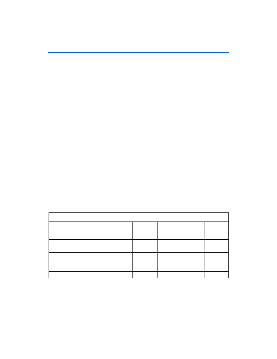
Table 3–4 shows the programming times for MAX II devices using
in-circuit testers to execute the algorithm vectors in hardware.
Software-based programming tools used with download cables are
slightly slower because of data processing and transfer limitations.
Table 3–4. MAX II Device Family Programming Times
Description
EPM240
EPM240G
EPM240Z
EPM570
EPM570G
EPM570Z
EPM1270
EPM1270G
EPM2210
EPM2210G
Unit
Erase + Program (1 MHz)
1.72
2.16
2.90
3.92
sec
Erase + Program (10 MHz)
1.65
1.99
2.58
3.40
sec
Verify (1 MHz)
0.09
0.17
0.30
0.49
sec
Verify (10 MHz)
0.01
0.02
0.03
0.05
sec
Complete Program Cycle (1 MHz)
1.81
2.33
3.20
4.41
sec
Complete Program Cycle (10 MHz)
1.66
2.01
2.61
3.45
sec
相关PDF资料 |
PDF描述 |
|---|---|
| EPM2210GF256A5N | FLASH PLD, PBGA256 |
| EPM2210GF324A3N | FLASH PLD, PBGA324 |
| EPM2210GF324A4N | FLASH PLD, PBGA324 |
| EPM2210GF324A5N | FLASH PLD, PBGA324 |
| EPM7064BFC100-3 | EE PLD, 3.5 ns, PBGA100 |
相关代理商/技术参数 |
参数描述 |
|---|---|
| EPM2210GF256C3 | 功能描述:CPLD - 复杂可编程逻辑器件 CPLD - MAX II 1700 Macro 204 IO RoHS:否 制造商:Lattice 系列: 存储类型:EEPROM 大电池数量:128 最大工作频率:333 MHz 延迟时间:2.7 ns 可编程输入/输出端数量:64 工作电源电压:3.3 V 最大工作温度:+ 90 C 最小工作温度:0 C 封装 / 箱体:TQFP-100 |
| EPM2210GF256C3N | 功能描述:CPLD - 复杂可编程逻辑器件 CPLD - MAX II 1700 Macro 204 IO RoHS:否 制造商:Lattice 系列: 存储类型:EEPROM 大电池数量:128 最大工作频率:333 MHz 延迟时间:2.7 ns 可编程输入/输出端数量:64 工作电源电压:3.3 V 最大工作温度:+ 90 C 最小工作温度:0 C 封装 / 箱体:TQFP-100 |
| EPM2210GF256C4 | 功能描述:CPLD - 复杂可编程逻辑器件 CPLD - MAX II 1700 Macro 204 IO RoHS:否 制造商:Lattice 系列: 存储类型:EEPROM 大电池数量:128 最大工作频率:333 MHz 延迟时间:2.7 ns 可编程输入/输出端数量:64 工作电源电压:3.3 V 最大工作温度:+ 90 C 最小工作温度:0 C 封装 / 箱体:TQFP-100 |
| EPM2210GF256C4N | 功能描述:CPLD - 复杂可编程逻辑器件 CPLD - MAX II 1700 Macro 204 IO RoHS:否 制造商:Lattice 系列: 存储类型:EEPROM 大电池数量:128 最大工作频率:333 MHz 延迟时间:2.7 ns 可编程输入/输出端数量:64 工作电源电压:3.3 V 最大工作温度:+ 90 C 最小工作温度:0 C 封装 / 箱体:TQFP-100 |
| EPM2210GF256C5 | 功能描述:CPLD - 复杂可编程逻辑器件 CPLD - MAX II 1700 Macro 204 IO RoHS:否 制造商:Lattice 系列: 存储类型:EEPROM 大电池数量:128 最大工作频率:333 MHz 延迟时间:2.7 ns 可编程输入/输出端数量:64 工作电源电压:3.3 V 最大工作温度:+ 90 C 最小工作温度:0 C 封装 / 箱体:TQFP-100 |
发布紧急采购,3分钟左右您将得到回复。