- 您现在的位置:买卖IC网 > PDF目录295888 > EPM2210GF256A4N (ALTERA CORP) FLASH PLD, PBGA256 PDF资料下载
参数资料
| 型号: | EPM2210GF256A4N |
| 厂商: | ALTERA CORP |
| 元件分类: | PLD |
| 英文描述: | FLASH PLD, PBGA256 |
| 封装: | 17 X 17 MM, 1 MM PITCH, LEAD FREE, FBGA-256 |
| 文件页数: | 80/108页 |
| 文件大小: | 1342K |
| 代理商: | EPM2210GF256A4N |
第1页第2页第3页第4页第5页第6页第7页第8页第9页第10页第11页第12页第13页第14页第15页第16页第17页第18页第19页第20页第21页第22页第23页第24页第25页第26页第27页第28页第29页第30页第31页第32页第33页第34页第35页第36页第37页第38页第39页第40页第41页第42页第43页第44页第45页第46页第47页第48页第49页第50页第51页第52页第53页第54页第55页第56页第57页第58页第59页第60页第61页第62页第63页第64页第65页第66页第67页第68页第69页第70页第71页第72页第73页第74页第75页第76页第77页第78页第79页当前第80页第81页第82页第83页第84页第85页第86页第87页第88页第89页第90页第91页第92页第93页第94页第95页第96页第97页第98页第99页第100页第101页第102页第103页第104页第105页第106页第107页第108页
Altera Corporation
5–3
July 2008
MAX II Device Handbook, Volume 1
DC and Switching Characteristics
Programming/Erasure Specifications
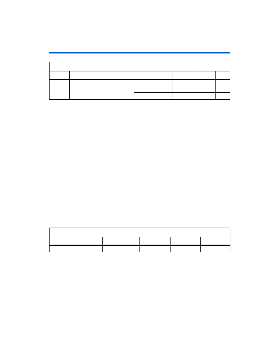
Table 5–3 shows the MAX II device family programming/erasure
specifications.
TJ
Operating junction temperature
Commercial range (5)
085
°C
Industrial range
–40
100
°C
Extended range (6)
–40
125
°C
Notes to Table 5–2
:
(1)
MAX II device in-system programming and/or user flash memory (UFM) programming via JTAG or logic array
is not guaranteed outside the recommended operating conditions (for example, if brown-out occurs in the system
during a potential write/program sequence to the UFM, users are recommended to read back UFM contents and
verify against the intended write data).
(2)
Minimum DC input is –0.5 V. During transitions, the inputs may undershoot to –2.0 V for input currents less than
100 mA and periods shorter than 20 ns.
(3)
During transitions, the inputs may overshoot to the voltages shown in the following table based upon input duty
cycle. The DC case is equivalent to 100% duty cycle. For more information about 5.0-V tolerance, refer to the Using
MAX II Devices in Multi-Voltage Systems chapter in the MAX II Device Handbook.
VIN
Max. Duty Cycle
4.0 V
100% (DC)
4.1
90%
4.2
50%
4.3
30%
4.4
17%
4.5
10%
(4)
All pins, including clock, I/O, and JTAG pins, may be driven before VCCINT and VCCIO are powered.
(5)
MAX IIZ devices are only available in the commercial temperature range.
(6)
For the extended temperature range of 100 to 125 C, MAX II UFM programming (erase/write) is only supported
via the JTAG interface. UFM programming via the logic array interface is not guaranteed in this range.
Table 5–2. MAX II Device Recommended Operating Conditions (Part 2 of 2)
Symbol
Parameter
Conditions
Minimum
Maximum
Unit
Table 5–3. MAX II Device Programming/Erasure Specifications
Parameter
Minimum
Typical
Maximum
Unit
Erase and reprogram cycles
—
100 (1)
Cycles
Note to Table 5–3
(1)
This specification applies to the UFM and configuration flash memory (CFM) blocks.
相关PDF资料 |
PDF描述 |
|---|---|
| EPM2210GF256A5N | FLASH PLD, PBGA256 |
| EPM2210GF324A3N | FLASH PLD, PBGA324 |
| EPM2210GF324A4N | FLASH PLD, PBGA324 |
| EPM2210GF324A5N | FLASH PLD, PBGA324 |
| EPM7064BFC100-3 | EE PLD, 3.5 ns, PBGA100 |
相关代理商/技术参数 |
参数描述 |
|---|---|
| EPM2210GF256C3 | 功能描述:CPLD - 复杂可编程逻辑器件 CPLD - MAX II 1700 Macro 204 IO RoHS:否 制造商:Lattice 系列: 存储类型:EEPROM 大电池数量:128 最大工作频率:333 MHz 延迟时间:2.7 ns 可编程输入/输出端数量:64 工作电源电压:3.3 V 最大工作温度:+ 90 C 最小工作温度:0 C 封装 / 箱体:TQFP-100 |
| EPM2210GF256C3N | 功能描述:CPLD - 复杂可编程逻辑器件 CPLD - MAX II 1700 Macro 204 IO RoHS:否 制造商:Lattice 系列: 存储类型:EEPROM 大电池数量:128 最大工作频率:333 MHz 延迟时间:2.7 ns 可编程输入/输出端数量:64 工作电源电压:3.3 V 最大工作温度:+ 90 C 最小工作温度:0 C 封装 / 箱体:TQFP-100 |
| EPM2210GF256C4 | 功能描述:CPLD - 复杂可编程逻辑器件 CPLD - MAX II 1700 Macro 204 IO RoHS:否 制造商:Lattice 系列: 存储类型:EEPROM 大电池数量:128 最大工作频率:333 MHz 延迟时间:2.7 ns 可编程输入/输出端数量:64 工作电源电压:3.3 V 最大工作温度:+ 90 C 最小工作温度:0 C 封装 / 箱体:TQFP-100 |
| EPM2210GF256C4N | 功能描述:CPLD - 复杂可编程逻辑器件 CPLD - MAX II 1700 Macro 204 IO RoHS:否 制造商:Lattice 系列: 存储类型:EEPROM 大电池数量:128 最大工作频率:333 MHz 延迟时间:2.7 ns 可编程输入/输出端数量:64 工作电源电压:3.3 V 最大工作温度:+ 90 C 最小工作温度:0 C 封装 / 箱体:TQFP-100 |
| EPM2210GF256C5 | 功能描述:CPLD - 复杂可编程逻辑器件 CPLD - MAX II 1700 Macro 204 IO RoHS:否 制造商:Lattice 系列: 存储类型:EEPROM 大电池数量:128 最大工作频率:333 MHz 延迟时间:2.7 ns 可编程输入/输出端数量:64 工作电源电压:3.3 V 最大工作温度:+ 90 C 最小工作温度:0 C 封装 / 箱体:TQFP-100 |
发布紧急采购,3分钟左右您将得到回复。