- 您现在的位置:买卖IC网 > PDF目录16581 > EVAL-AD5171DBZ (Analog Devices Inc)BOARD EVAL FOR AD5171DBZ PDF资料下载
参数资料
| 型号: | EVAL-AD5171DBZ |
| 厂商: | Analog Devices Inc |
| 文件页数: | 10/24页 |
| 文件大小: | 0K |
| 描述: | BOARD EVAL FOR AD5171DBZ |
| 标准包装: | 1 |
| 系列: | * |
AD5171
Rev. D | Page 18 of 24
the instruction byte, the last byte in the write mode is the data
byte. Data is transmitted over the serial bus in sequences of nine
clock pulses (eight data bits followed by an acknowledge bit).
The transitions on the SDA line must occur during the low
period of SCL and remain stable during the high period of SCL
(see Figure 35).
In read mode, the data byte follows immediately after the
acknowledgment of the slave address byte. Data is transmitted over
the serial bus in sequences of nine clock pulses (note the slight
difference from the write mode; there are eight data bits followed
by a no acknowledge bit). Similarly, the transitions on the SDA
line must occur during the low period of SCL and remain stable
during the high period of SCL (see Figure 37).
When all data bits are read or written, a stop condition is
established by the master. A stop condition is defined as a low-
to-high transition on the SDA line while SCL is high. In the
write mode, the master pulls the SDA line high during the 10th
clock pulse to establish a stop condition (see Figure 35 and
Figure 36). In the read mode, the master issues a no acknowledge
for the 9th clock pulse, that is, the SDA line remains high. The
master then brings the SDA line low before the 10th clock pulse,
which goes high to establish a stop condition (see Figure 37).
A repeated write function gives the user flexibility to update the
RDAC output a number of times, except after permanent
programming, addressing, and instructing the part only once.
During the write cycle, each data byte updates the RDAC output.
For example, after the RDAC has acknowledged its slave address
and instruction bytes, the RDAC output updates after these two
bytes. If another byte is written to the RDAC while it is still
addressed to a specific slave device with the same instruction,
this byte updates the output of the selected slave device. If
different instructions are needed, the write mode has to be
started with a new slave address, instruction, and data bytes.
Similarly, a repeated read function of the RDAC is also allowed.
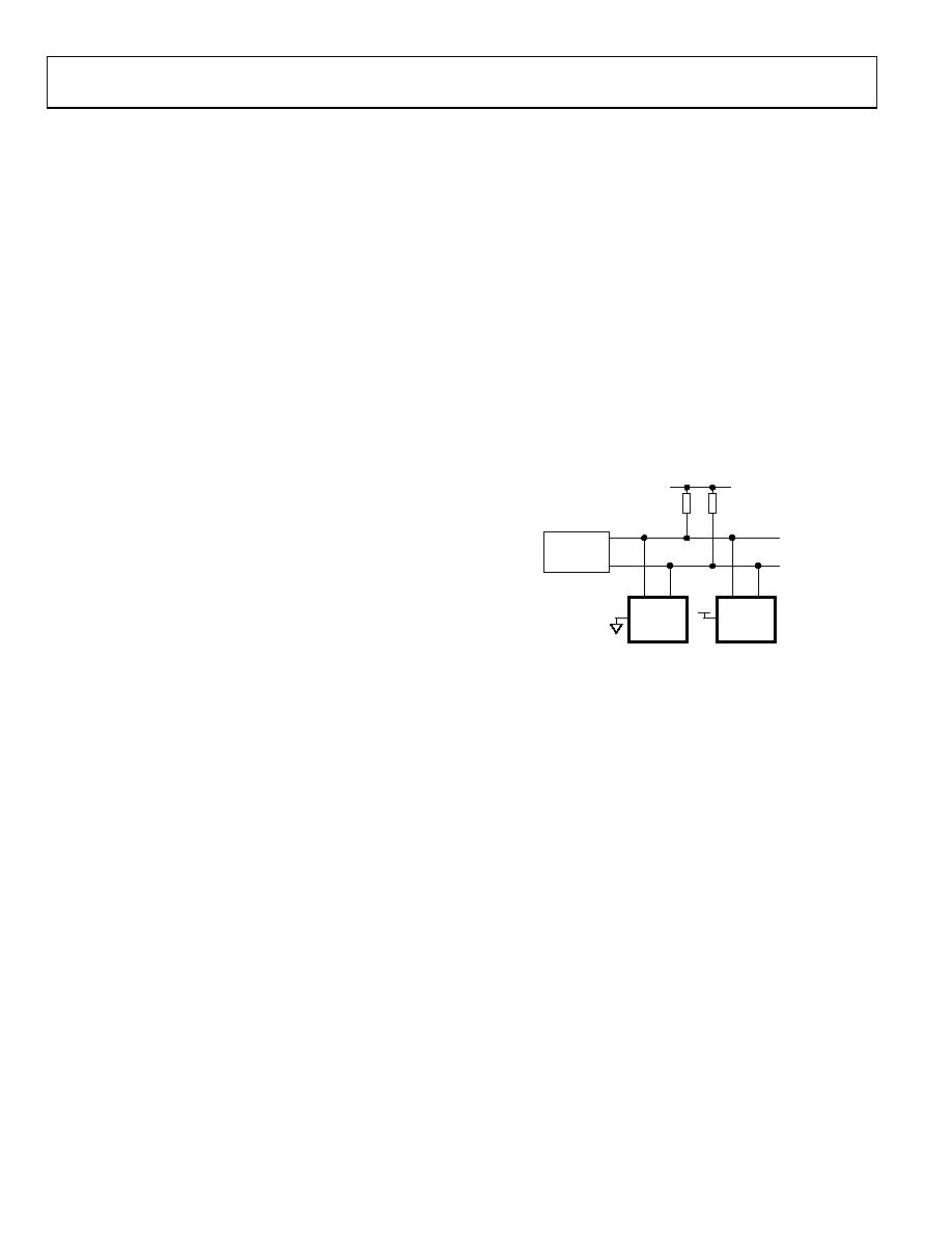
CONTROLLING TWO DEVICES ON ONE BUS
Figure 38 shows two AD5171 devices on the same serial bus.
Each has a different slave address because the state of each AD0
pin is different, which allows each device to be independently
operated. The master device output bus line drivers are open-
drain pull-downs in a fully I2C-compatible interface.
MASTER
SDA SCL
AD0
AD5171
SDA SCL
AD0
AD5171
SDA
SCL
5V
Rp
5V
03
43
7-
0
38
Figure 38. Two AD5171 Devices on One Bus
相关PDF资料 |
PDF描述 |
|---|---|
| CI100505-68NJ | INDUCTOR MULTI LAYER CHIP 68NH |
| EVAL-ADG884EBZ | BOARD EVAL FOR ADG884 |
| EEM43DRKN-S13 | CONN EDGECARD 86POS .156 EXTEND |
| EEM43DRKH-S13 | CONN EDGECARD 86POS .156 EXTEND |
| EVAL-AD5204SDZ | BOARD EVAL FOR AD5204 |
相关代理商/技术参数 |
参数描述 |
|---|---|
| EVAL-AD5172SDZ | 功能描述:BOARD EVAL FOR AD5172 RoHS:是 类别:编程器,开发系统 >> 评估演示板和套件 系列:- 标准包装:1 系列:- 主要目的:电信,线路接口单元(LIU) 嵌入式:- 已用 IC / 零件:IDT82V2081 主要属性:T1/J1/E1 LIU 次要属性:- 已供物品:板,电源,线缆,CD 其它名称:82EBV2081 |
| EVAL-AD5204SDZ | 功能描述:BOARD EVAL FOR AD5204 RoHS:是 类别:编程器,开发系统 >> 评估演示板和套件 系列:* 标准包装:1 系列:- 主要目的:电信,线路接口单元(LIU) 嵌入式:- 已用 IC / 零件:IDT82V2081 主要属性:T1/J1/E1 LIU 次要属性:- 已供物品:板,电源,线缆,CD 其它名称:82EBV2081 |
| EVAL-AD5222SDZ | 功能描述:BOARD EVAL FOR AD5222 RoHS:是 类别:编程器,开发系统 >> 评估演示板和套件 系列:* 标准包装:1 系列:- 主要目的:电信,线路接口单元(LIU) 嵌入式:- 已用 IC / 零件:IDT82V2081 主要属性:T1/J1/E1 LIU 次要属性:- 已供物品:板,电源,线缆,CD 其它名称:82EBV2081 |
| EVAL-AD5228EBZ | 功能描述:BOARD EVAL FOR AD5228 DGTL POT RoHS:是 类别:编程器,开发系统 >> 评估演示板和套件 系列:- 标准包装:1 系列:- 主要目的:电信,线路接口单元(LIU) 嵌入式:- 已用 IC / 零件:IDT82V2081 主要属性:T1/J1/E1 LIU 次要属性:- 已供物品:板,电源,线缆,CD 其它名称:82EBV2081 |
| EVAL-AD5232-10EBZ | 功能描述:BOARD EVALUATION FOR AD5232-10 RoHS:是 类别:编程器,开发系统 >> 评估演示板和套件 系列:- 标准包装:1 系列:- 主要目的:电信,线路接口单元(LIU) 嵌入式:- 已用 IC / 零件:IDT82V2081 主要属性:T1/J1/E1 LIU 次要属性:- 已供物品:板,电源,线缆,CD 其它名称:82EBV2081 |
发布紧急采购,3分钟左右您将得到回复。