- 您现在的位置:买卖IC网 > PDF目录16581 > EVAL-AD5171DBZ (Analog Devices Inc)BOARD EVAL FOR AD5171DBZ PDF资料下载
参数资料
| 型号: | EVAL-AD5171DBZ |
| 厂商: | Analog Devices Inc |
| 文件页数: | 8/24页 |
| 文件大小: | 0K |
| 描述: | BOARD EVAL FOR AD5171DBZ |
| 标准包装: | 1 |
| 系列: | * |
AD5171
Rev. D | Page 16 of 24
CONTROLLING THE AD5171
There are two ways of controlling the AD5171. Users can either
program the devices with computer software or employ external
I2C controllers.
SOFTWARE PROGRAMMING
Due to the advantage of the one-time programmable feature,
users may consider programming the device in the factory
before shipping it to the end users. Analog Devices offers device
programming software that can be implemented in the factory
on PCs running Windows 95 to Windows XP platforms. As a
result, external controllers are not required, which significantly
reduces development time.
The program is an executable file that does not require the user
to know any programming languages or programming skills. It
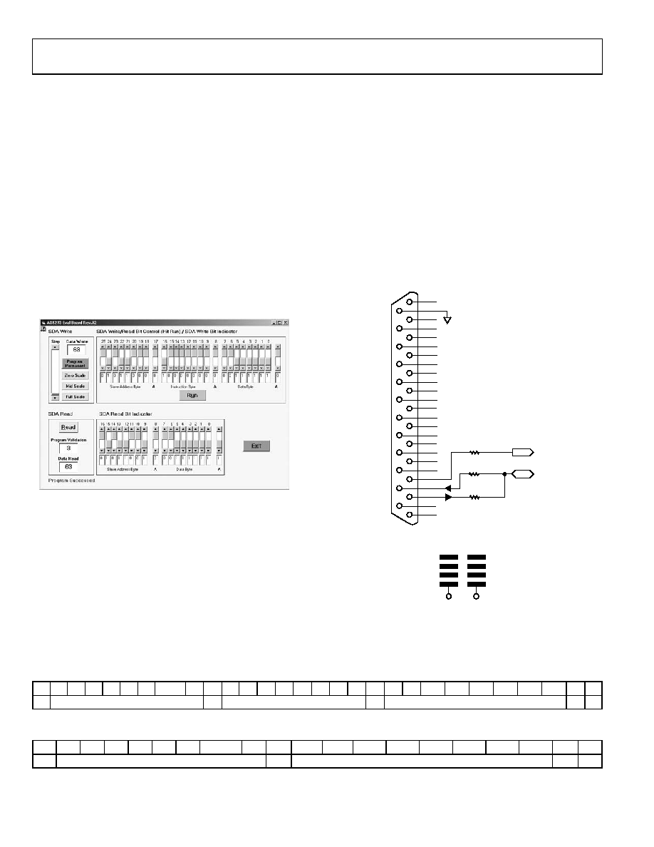
is easy to set up and use. Figure 32 shows the software interface.
The software can be downloaded from the AD5171 product page.
03
43
7-
0
32
Figure 32. Software Interface
Write
The AD5171 starts at midscale after power-up prior to the OTP
programming. To increment or decrement the resistance, move
the scrollbar on the left. To write any specific values, use the bit
pattern control in the upper screen and click Run. The format
of writing data to the device is shown in Table 8. Once the
desired setting is found, click Program Permanent to blow the
internal fuse links for permanent setting. The user can also set
the programming bit pattern in the upper screen and click Run
to achieve the same result.
Read
To read the validation bits and data from the device, click Read.
The user may also set the bit pattern in the upper screen and
click Run. The format of reading data out from the device is
shown in Table 9.
DEVICE PROGRAMMING
To apply the device programming software in the factory, users
need to modify a parallel port cable and configure Pin 2, Pin 3,
Pin 15, and Pin 25 for SDA_write, SCL, SDA_read, and DGND,
respectively, for the control signals (see Figure 33). In addition,
lay out the PCB of the AD5171 with SCL and SDA pads, as
shown in Figure 34, such that pogo pins can be inserted for the
factory programming.
13
25
12
24
11
23
10
22
9
21
8
20
7
19
6
18
5
17
4
16
3
15
2
14
1
SCL
R3
100
R2
100
R1
100
SDA
READ
WRITE
0
34
37
-03
3
Figure 33. Parallel Port Connection: Pin 2 = SDA_write, Pin 3 = SCL,
Pin 15 = SDA_read, and Pin 25 = DGND
W
VDD
GND
SCL
A
B
AD0
SDA
04
10
4
-03
4
Figure 34. Recommended AD5171 PCB Layout
Table 8. SDA Write Mode Bit Format
S
0
1
0
1
0
AD0
0
A
T
X
A
X
D5
D4
D3
D2
D1
D0
A
P
Slave Address Byte
Instruction Byte
Data Byte
Table 9. SDA Read Mode Bit Format
S
0
1
0
1
0
AD0
1
A
E1
E0
D5
D4
D3
D2
D1
D0
A
P
Slave Address Byte
Data Byte
相关PDF资料 |
PDF描述 |
|---|---|
| CI100505-68NJ | INDUCTOR MULTI LAYER CHIP 68NH |
| EVAL-ADG884EBZ | BOARD EVAL FOR ADG884 |
| EEM43DRKN-S13 | CONN EDGECARD 86POS .156 EXTEND |
| EEM43DRKH-S13 | CONN EDGECARD 86POS .156 EXTEND |
| EVAL-AD5204SDZ | BOARD EVAL FOR AD5204 |
相关代理商/技术参数 |
参数描述 |
|---|---|
| EVAL-AD5172SDZ | 功能描述:BOARD EVAL FOR AD5172 RoHS:是 类别:编程器,开发系统 >> 评估演示板和套件 系列:- 标准包装:1 系列:- 主要目的:电信,线路接口单元(LIU) 嵌入式:- 已用 IC / 零件:IDT82V2081 主要属性:T1/J1/E1 LIU 次要属性:- 已供物品:板,电源,线缆,CD 其它名称:82EBV2081 |
| EVAL-AD5204SDZ | 功能描述:BOARD EVAL FOR AD5204 RoHS:是 类别:编程器,开发系统 >> 评估演示板和套件 系列:* 标准包装:1 系列:- 主要目的:电信,线路接口单元(LIU) 嵌入式:- 已用 IC / 零件:IDT82V2081 主要属性:T1/J1/E1 LIU 次要属性:- 已供物品:板,电源,线缆,CD 其它名称:82EBV2081 |
| EVAL-AD5222SDZ | 功能描述:BOARD EVAL FOR AD5222 RoHS:是 类别:编程器,开发系统 >> 评估演示板和套件 系列:* 标准包装:1 系列:- 主要目的:电信,线路接口单元(LIU) 嵌入式:- 已用 IC / 零件:IDT82V2081 主要属性:T1/J1/E1 LIU 次要属性:- 已供物品:板,电源,线缆,CD 其它名称:82EBV2081 |
| EVAL-AD5228EBZ | 功能描述:BOARD EVAL FOR AD5228 DGTL POT RoHS:是 类别:编程器,开发系统 >> 评估演示板和套件 系列:- 标准包装:1 系列:- 主要目的:电信,线路接口单元(LIU) 嵌入式:- 已用 IC / 零件:IDT82V2081 主要属性:T1/J1/E1 LIU 次要属性:- 已供物品:板,电源,线缆,CD 其它名称:82EBV2081 |
| EVAL-AD5232-10EBZ | 功能描述:BOARD EVALUATION FOR AD5232-10 RoHS:是 类别:编程器,开发系统 >> 评估演示板和套件 系列:- 标准包装:1 系列:- 主要目的:电信,线路接口单元(LIU) 嵌入式:- 已用 IC / 零件:IDT82V2081 主要属性:T1/J1/E1 LIU 次要属性:- 已供物品:板,电源,线缆,CD 其它名称:82EBV2081 |
发布紧急采购,3分钟左右您将得到回复。