- 您现在的位置:买卖IC网 > PDF目录16581 > EVAL-AD5247DBZ (Analog Devices Inc)BOARD EVAL FOR AD5247DBZ PDF资料下载
参数资料
| 型号: | EVAL-AD5247DBZ |
| 厂商: | Analog Devices Inc |
| 文件页数: | 6/20页 |
| 文件大小: | 0K |
| 描述: | BOARD EVAL FOR AD5247DBZ |
| 标准包装: | 1 |
| 系列: | * |
AD5247
Data Sheet
Rev. F | Page 14 of 20
THEORY OF OPERATION
The AD5247 is a 128-position, digitally-controlled variable
resistor (VR) device. An internal power-on preset places the
wiper at midscale during power-on, which simplifies the
default condition recovery at power-up.
PROGRAMMING THE VARIABLE RESISTOR
Rheostat Operation
The nominal resistance (RAB) of the RDAC between Terminal A
and Terminal B is available in 5 k, 10 k, 50 k, and 100 k. The
final two or three digits of the part number determine the nominal
resistance value; for example, 10 k = 10 and 50 k = 50. The
RAB of the VR has 128 contact points accessed by the wiper
terminal, plus the B terminal contact. The 7-bit data in the
RDAC latch is decoded to select one of the 128 possible settings.
Assuming a 10 k part is used, the wiper’s first connection starts
at the B terminal for Data 0x00. Because there is a 50 wiper
contact resistance, such a connection yields a minimum of 100
(2 × 50 ) resistance between Terminal W and Terminal B. The
second connection is the first tap point, corresponding to 178
(RWB = RAB/128 + RW = 78 + 2 × 50 ) for Data 0x01. The third
connection is the next tap point, representing 256 (2 × 78
+ 2 × 50 ) for Data 0x02, and so on. Each LSB data value increase
moves the wiper up the resistor ladder until the last tap point is
reached at 10,100 (RAB + 2 × RW).
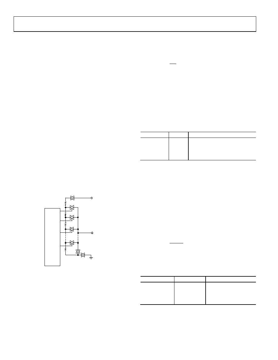
Figure 35 shows a simplified diagram of the equivalent RDAC
circuit where the last resistor string is not accessed.
Bx
Wx
Ax
D6
D4
D5
D2
D3
D1
D0
RDAC
LATCH
AND
DECODER
RS
03876-
034
Figure 35. AD5247 Equivalent RDAC Circuit
The general equation determining the digitally programmed
output resistance between W and B is
W
AB
WB
R
D
(D)
R
×
+
×
=
2
128
(1)
where:
D is the decimal equivalent of the binary code loaded in the
7-bit RDAC register.
RAB is the end-to-end resistance.
RW is the wiper resistance contributed by the on resistance of
the internal switch.
In summary, if RAB = 10 k and the Terminal A is open-circuited,
RDAC latch codes.
Table 9. Codes and Corresponding RWB Resistance
D (Decimal)
RWB ()
Output State
127
10,072
Full scale (RAB + 2 × RW)
64
5150
Midscale
1
228
1 LSB
0
150
Zero scale (wiper contact resistance)
Note that in the zero-scale condition, a finite resistance of
100 between Terminal W and Terminal B is present. Care
should be taken to limit the current flow between W and B in
this state to a maximum pulse current of no more than 20 mA.
Otherwise, degradation or possible destruction of the internal
switch contact can occur.
Similar to the mechanical potentiometer, the resistance of
the RDAC between Wiper W and Terminal A also produces a
digitally controlled complementary resistance, RWA. When
these terminals are used, the Terminal B can be opened. Set the
resistance value for RWA to start at a maximum value of resistance
and to decrease the data loaded in the latch increases in value.
The general equation for this operation is
W
AB
WA
R
D
(D)
R
×
+
×
=
2
128
(2)
If RAB = 10 k and the B terminal is open-circuited, the output
latch codes.
Table 10. Codes and Corresponding RWA Resistance
D (Decimal)
RWA ()
Output State
127
228
Full scale
64
5150
Midscale
1
10,071
1 LSB
0
10,150
Zero scale
Typical device-to-device matching is process lot dependent
and can vary by up to ±30%. Because the resistance element
is processed in thin film technology, the change in RAB with
temperature has a very low 45 ppm/°C temperature coefficient.
相关PDF资料 |
PDF描述 |
|---|---|
| EEM43DSEN-S13 | CONN EDGECARD 86POS .156 EXTEND |
| CI100505-82NJ | INDUCTOR MULTI LAYER CHIP 82NH |
| CI160808-1N0D | INDUCTOR MULTI LAYER CHIP 1.0NH |
| EEM43DSEH-S13 | CONN EDGECARD 86POS .156 EXTEND |
| GBM24DRTI | CONN EDGECARD 48POS DIP .156 SLD |
相关代理商/技术参数 |
参数描述 |
|---|---|
| EVAL-AD5252EBZ | 功能描述:BOARD EVAL FOR AD5252 RoHS:是 类别:编程器,开发系统 >> 评估演示板和套件 系列:- 产品培训模块:Obsolescence Mitigation Program 标准包装:1 系列:- 主要目的:电源管理,电池充电器 嵌入式:否 已用 IC / 零件:MAX8903A 主要属性:1 芯锂离子电池 次要属性:状态 LED 已供物品:板 |
| EVAL-AD5252SDZ | 功能描述:BOARD EVAL FOR AD5252 RoHS:是 类别:编程器,开发系统 >> 评估演示板和套件 系列:- 标准包装:1 系列:- 主要目的:电信,线路接口单元(LIU) 嵌入式:- 已用 IC / 零件:IDT82V2081 主要属性:T1/J1/E1 LIU 次要属性:- 已供物品:板,电源,线缆,CD 其它名称:82EBV2081 |
| EVAL-AD5254EBZ | 制造商:Analog Devices 功能描述:EVALUATION BOARD - Boxed Product (Development Kits) |
| EVAL-AD5254SDZ | 功能描述:BOARD EVAL FOR AD5254 RoHS:是 类别:编程器,开发系统 >> 评估演示板和套件 系列:- 标准包装:1 系列:- 主要目的:电信,线路接口单元(LIU) 嵌入式:- 已用 IC / 零件:IDT82V2081 主要属性:T1/J1/E1 LIU 次要属性:- 已供物品:板,电源,线缆,CD 其它名称:82EBV2081 |
| EVAL-AD5258DBZ | 功能描述:BOARD EVAL FOR AD5258DBZ RoHS:否 类别:编程器,开发系统 >> 评估演示板和套件 系列:* 标准包装:1 系列:- 主要目的:电信,线路接口单元(LIU) 嵌入式:- 已用 IC / 零件:IDT82V2081 主要属性:T1/J1/E1 LIU 次要属性:- 已供物品:板,电源,线缆,CD 其它名称:82EBV2081 |
发布紧急采购,3分钟左右您将得到回复。